Thermal Interface Materials for AI Hardware: Selection Guide
Choosing thermal interface materials for AI hardware: compare pads, gap fillers, grease, and PCM by conductivity, thickness, and pressure in five steps.
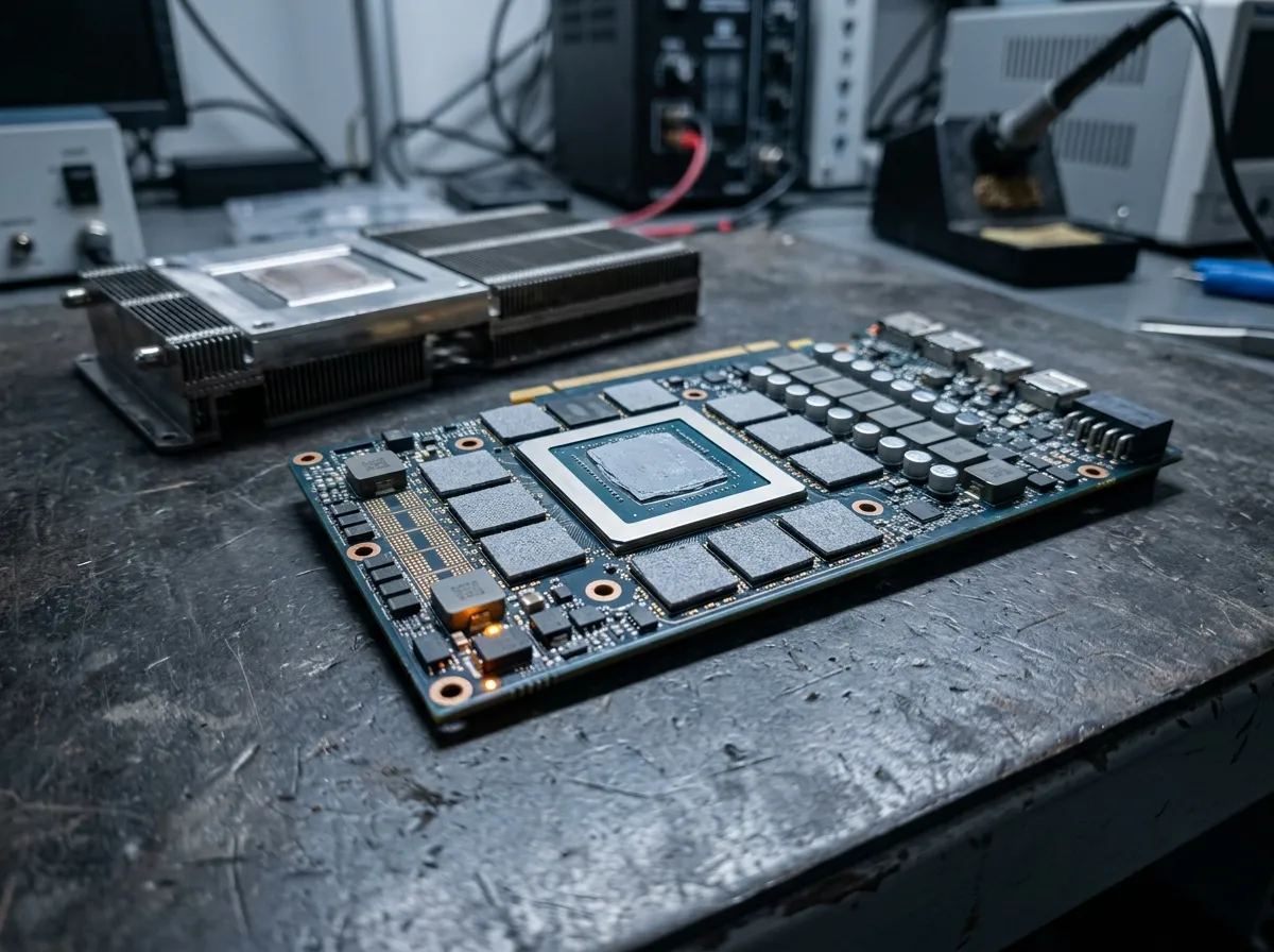
Why AI Hardware Pushes Thermal Interface Materials to Their Limits
Flagship AI accelerators now draw 700–1,000 W, and next-generation training silicon is expected to exceed 1,200 W per device as 2.5D and 3D packaging stack more compute into the same footprint. In that regime the thermal interface material stops being a detail: a 2025 review of thermal interface materials in Materials Today Physics notes that these materials exist to keep heat moving between power-hungry components and their heat sinks — and the interface between silicon and its cooling hardware has become one of the largest remaining thermal resistances in the system.
That interface is where thermal interface materials for AI hardware earn their keep. No machined surface is flat at the microscopic scale; without a filler, the die-to-heatsink gap traps air, which conducts heat roughly 40–300 times worse than typical TIM formulations. The material's only job is to displace that air and create a continuous thermal path — but on a kilowatt-class accelerator, a poorly chosen material can add tens of degrees Celsius at the junction, throttle the part, or fail inside the warranty window.
This guide gives you a spec-first way to choose. Instead of starting with the highest W/m·K number you can find, you define the thermal and mechanical constraints of your design, screen the material classes that can realistically meet them, verify the datasheet, and qualify a sample. The whole family of options — pads, gap fillers, grease, phase change materials, liquid metal, carbon fiber — fits inside that workflow. For the full set of resources on this topic, start at our thermal materials for data centers and AI servers hub.
Five Specs That Actually Decide a TIM for AI Hardware
Datasheets list a dozen numbers, but five of them decide almost every AI-hardware selection. The other seven are either derivatives of these or marketing.
Thermal conductivity (W/m·K). The headline number, and the most misleading one on the sheet. It describes the bulk material's ability to conduct heat — useful for comparing within one material family, useless for comparing pads against grease. If you need the definition and the measurement caveats, our explainer on what W/m·K actually measures covers the details.
Thermal resistance and impedance. The number that matters in the real assembly. Thermal resistance folds in the thickness (bond line), the contact pressure, and the two interface surfaces — so a 16 W/m·K pad at 2 mm thick can lose to a 5 W/m·K pad at 0.5 mm. The difference between resistance and impedance, and why suppliers quote one or the other, is worth reading in our thermal resistance versus impedance comparison.
Hardness and compressibility (Shore OO). A pad that cannot deform under your mounting pressure leaves air pockets exactly where you need contact. Soft pads (10–40 Shore OO) conform at low pressure but may squeeze out of tight gaps; hard pads carry loads but need real clamping force. Your assembly's pressure budget is the constraint that decides this spec.
Dielectric strength and electrical behavior. Most AI-hardware interfaces need electrical insulation (dielectric strength in kV/mm), because the heat sink or cold plate may sit at a different potential than the die. Conductive pads and liquid metal are the exceptions — they are chosen deliberately, for grounding or EMI, not by accident.
Reliability under real conditions. Thermal cycling, pump-out (grease migrating away under repeated expansion), oil bleed, and outgassing all erode performance over months. A material that wins on paper but pumps out of a direct-die interface after 10,000 cycles is a field failure.
Material Classes: Where Each TIM Wins on AI Hardware
Once the five specs are on paper, the material class almost selects itself. Here is the shortlist, with the situations where each class wins on AI hardware:
| Material | Typical conductivity | AI hardware sweet spot | Watch out for |
|---|---|---|---|
| Thermal pad | 1–16 W/m·K | Large, uneven gaps; HBM/VRAM stacks; anything that needs rework | Fixed thickness; needs enough pressure to conform |
| Gap filler / gel | 1–12 W/m·K | Variable gaps, automated dispensing, cold-plate TIM2 | Cure time; dispensing equipment |
| Thermal grease / paste | 1–8 W/m·K | Thin bond lines with high clamping force; die-level TIM1 | Pump-out; mess; no rework tolerance |
| Phase change material (PCM) | 1–10 W/m·K | Die-level interfaces that must survive thermal cycling | Activation temperature; storage handling |
| Liquid metal | ~35 W/m·K | Extreme heat flux, research/evaluation builds | Corrosion of aluminum/copper; application skill |
| Carbon fiber pad | 9–25 W/m·K | Ultra-thin, low-pressure, silicone-free clean interfaces | Electrically conductive — not for insulated gaps |
| Thermal putty | 1–10 W/m·K | GPU service/replacement market; odd-shaped gaps | Less standardized; softer consistency |
Two boundary decisions come up constantly. The first is pad versus paste: if your design has a defined gap and needs rework, when a pad beats paste is the criterion. The second is gel versus pad versus PCM on die-level interfaces — the three-way tradeoff between conductivity, pressure, and longevity is mapped in our gap filler, pad, or phase change comparison.
If you are sourcing silicone pads, the realistic spec envelope is wider than most buyers assume. Silicone pad series such as ZIITEK's TIF line span 1.25–16 W/m·K at 0.25–12 mm thickness with 5–70 Shore OO hardness and UL 94 V-0 flame retardancy — which covers everything from thin VRAM pads to thick gap-filling slabs in one product family.
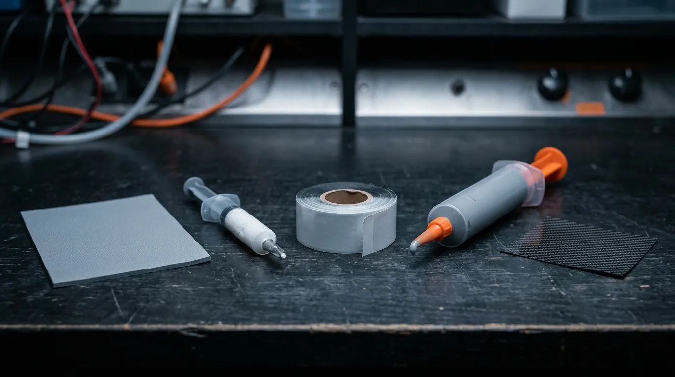
Thermal interface materials come in seven distinct formats; the selection is about matching format to gap, pressure, and thermal budget.
A Five-Step Selection Workflow for AI Hardware
This is the practical part: a repeatable way to screen thermal interface materials for AI hardware designs instead of comparing datasheets against each other blindly.
Step 1 — Define the heat path and the thermal budget. Draw the path from junction to ambient or coolant. Write down the maximum allowed junction temperature, the expected power, and the temperature of the sink side. The difference, divided by power, is your total allowed thermal resistance budget — the TIM has to fit inside a fraction of it.
Step 2 — Define the mechanical constraints. Measure the gap the material must fill, the tolerance on that gap, the mounting pressure available, and whether the assembly ever needs rework. Also note the environment: optical modules and clean assemblies disqualify silicone-based materials that outgas low-molecular-weight siloxanes.
Step 3 — Screen material classes against the constraints. Work down the table above. A defined gap with rework needs pads; a variable gap needs gel or putty; a clamped, thin, never-reworked die interface can use grease or PCM; a silicone-free requirement pushes you to carbon fiber or non-silicone pads. If the gap-filler route is winning, our guide to choosing a thermal gap filler walks through the gel-specific specs.
Step 4 — Verify the datasheet, don't read it. Two pads with the same W/m·K can differ by 3× in real resistance because of test conditions. Ask for the test method (ASTM D5470 is the industry baseline), the bond line thickness and pressure the number was measured at, and the unit — °C·in²/W and °C·cm²/W differ by 6.45× and get confused constantly.
Conductivity is a material property; resistance is a system property. The datasheet you can trust is the one that reports both.
Step 5 — Prototype, test, and qualify. Sample the finalists, measure with your real heat sink and your real clamping hardware, then run thermal cycling and aging. This is where suppliers with in-house formulation and die-cutting earn their keep — a die-cut pad to your exact footprint, delivered from the same process as production, removes a whole class of assembly surprises.

Liquid-cooled AI racks push more heat through cold-plate interfaces, which raises the bar for TIM2 materials under sustained clamping pressure.
Where Each TIM Goes on an AI Accelerator
Mapping the material classes to an actual accelerator makes the abstract specs concrete:
- Die to integrated heat spreader (TIM1): PCM or high-conductivity gel; liquid metal is being evaluated on leading-edge parts. Chip vendors publish their own requirements here — AMD's DS955 application note, for instance, specifies the thermal interface material for its Versal AI Edge parts. The thinnest bond line and highest conductivity live at this layer.
- Direct die to cold plate (TIM1.5/TIM2): high-conductivity gel or a conformable pad under substantial clamping pressure. With liquid cooling, this interface can become the single biggest resistance in the whole path — the cold plate is efficient, so the TIM is the bottleneck.
- HBM and VRAM stacks: softer, moderately conductive pads that conform to many small chips without crushing them. This is where most thermal pad for gpu replacements happen — the memory stacks sit under the same heat sink as the die.
- Power delivery stages (MOSFETs, VRMs): electrically insulative pads, because the pads sit directly on components at different potentials.
- NVMe and U.2 SSDs: thin pads (0.5–1 mm) sized to the controller and NAND packages — the thermal pad for ssd category — with enough compressibility to absorb stack-up tolerance.
- Optical modules and co-packaged optics: carbon fiber or silicone-free pads where siloxane outgassing would fog optics.
- Service and aftermarket GPU repair: thermal putty has become the default for odd-shaped gaps on disassembled cards, because it conforms without measuring the exact pad thickness first.
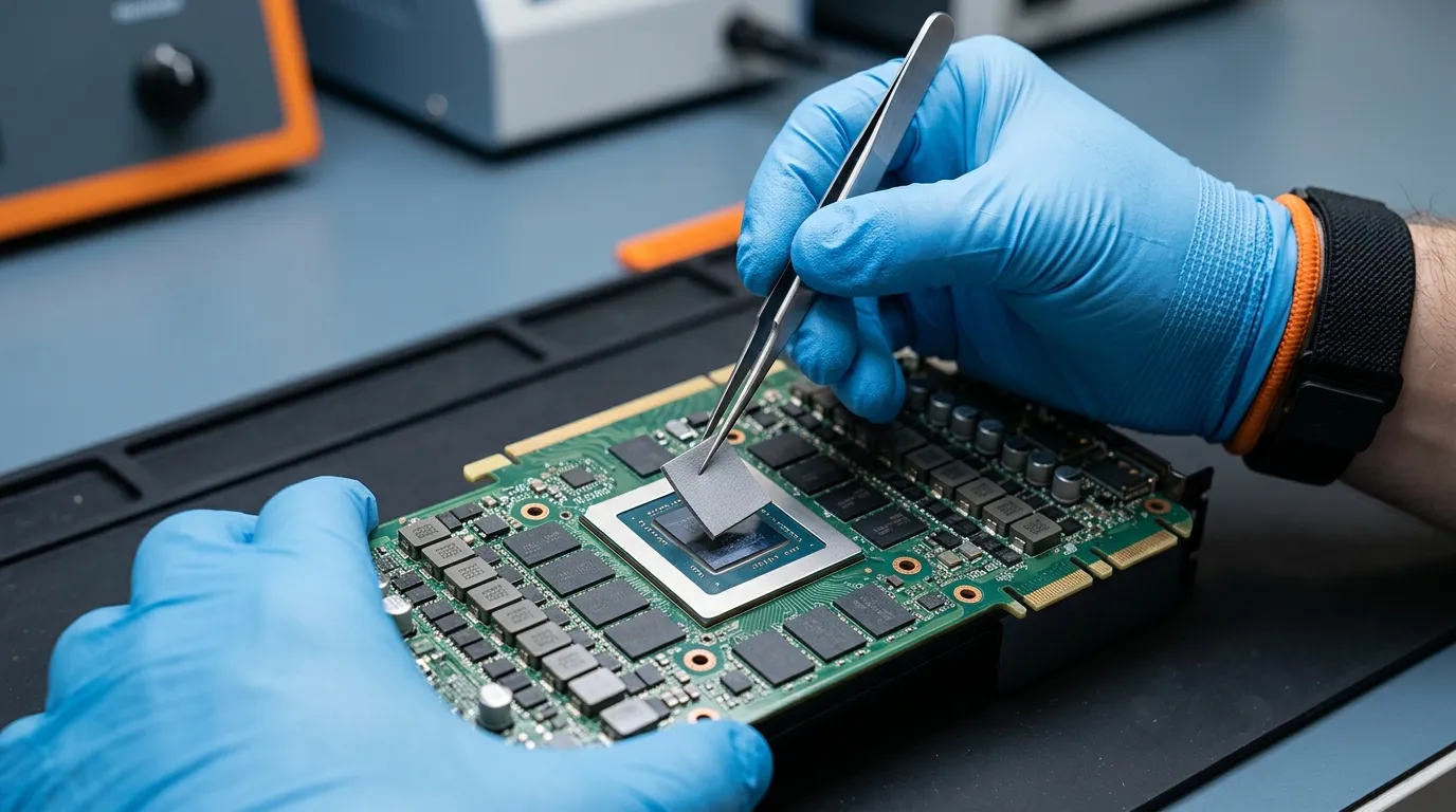
Die-cut pads to the exact component footprint remove the assembly-time guesswork that generic sheets introduce.
Common Specification Mistakes and What to Ask Your Supplier
The mistakes that survive into production are almost always the same five:
- Buying the highest W/m·K without checking bond line or pressure. The 16 W/m·K pad at 2 mm can lose to the 5 W/m·K pad at 0.5 mm.
- Trusting the datasheet number. Without the test conditions, the number is not comparable. Ask: which standard, what pressure, what bond line, what sample size.
- Ignoring pump-out and bleed on die-level interfaces. Grease that pumps out after thermal cycling turns a premium interface into an air gap. PCM and high-stability gels exist precisely for this failure mode.
- Forgetting silicone outgassing. In optical, sensor, or sealed assemblies, low-molecular-weight siloxanes from silicone pads and gels condense onto optics. Specify low-volatile or silicone-free materials up front.
- Not budgeting compression force. A hard pad that needs 100 psi of clamping when your cold plate delivers 30 psi is not "close enough" — it is a 2°C penalty hiding in the stack.
Compliance paperwork matters in the same way: for AI hardware bound for data centers and export markets, confirm the UL yellow card (ZIITEK's covers its pad and plastic families under file E331100), RoHS and REACH declarations, and, for automotive-adjacent designs, IATF 16949 traceability — before qualification, not after.
A practical close-out checklist, worth running against any shortlist before you order samples:
| Check | Why it matters |
|---|---|
| Datasheet states the test standard (ASTM D5470 or equivalent) and the exact pressure and bond line | Without the conditions, the resistance number is not comparable across suppliers |
| Conductivity and resistance values come from the same test sample | Mixed data points hide inconsistencies between a "headline" conductivity and a real resistance |
| UL file number exists for flame-rated materials; RoHS/REACH declarations are current and dated | Missing compliance blocks data-center and export shipments at qualification time |
| Aging or thermal-cycling data exists for die-level interfaces | Static conductivity tells you nothing about pump-out or degradation over 10,000 cycles |
| Supplier can die-cut or convert to your exact footprint with consistent batch tolerances | Generic sheets add assembly-time cutting and tolerance drift in production |
| Samples ship with the same process and formulation as production | A "lab-grade special" sample that differs from production batches invalidates your test results |
Getting the Right Thermal Interface Materials for AI Hardware
The workflow collapses into one sentence: define the thermal budget and mechanical constraints first, screen the material classes, verify the datasheet, then qualify a sample — in that order. If you start from the constraint side instead of the conductivity column, the right material class usually announces itself, and the remaining decision is a spec sheet comparison instead of a guess.
If your design has reached the datasheet stage, sending the working numbers is the fastest way to a shortlist. ZIITEK's engineering team works from the same five specs described here and can match or tune a material to your gap, pressure, and thermal budget — browse the thermal pad product family to see the range, or check the AI server thermal materials hub for the surrounding guides. The fundamentals guides on thermal conductivity and on resistance versus impedance are good reading while you wait for samples.