Graphite Heat Spreader Sheets for Thin Devices: A Guide
How to choose a graphite heat spreader sheet for thin consumer devices: anisotropy, natural vs synthetic graphite, thickness and adhesive, and supplier checks.
Why Thin Devices Need a Graphite Heat Spreader
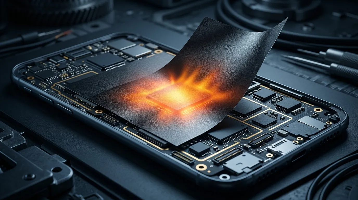
A flagship phone SoC can pull tens of watts in a burst, yet it sits inside an enclosure a few millimeters thick with no fan and very little metal to absorb the heat. Air does not help — it conducts at roughly 0.026 W/m·K — so the heat has to be moved by whatever solid path the design provides. The problem is geometry: the chip is a point source, and the only large surfaces available to shed heat, the midframe, the shield cans, the back cover, are centimeters away. A solid metal slug between them would be too heavy and too thick, and that point-source-to-large-surface gap is exactly what a graphite heat spreader is built to fill.
The material in question is a flexible graphite heat spreader: a thin sheet of compressed carbon that takes heat from the hotspot and spreads it sideways across a large area, turning the whole interior surface of the device into a radiator. The same class of material that keeps smartphones cool also appears in tablets, laptops, M.2 SSDs, VR headsets, OLED panels and set-top boxes — anywhere the enclosure is too thin for metal and too dense for airflow. It is one of the few thermal parts in a consumer device you can tune independently of the chip architecture, which is exactly why so many thermal teams treat the sheet selection as a real engineering decision.
Graphite earns that role through three properties no bulk metal matches at this thickness: extremely high in-plane conductivity (several times copper per unit weight), extreme thinness (many grades are 0.02–0.05 mm), and mechanical flexibility, so it can be wrapped around batteries and folded over stacked boards. If you are new to the surrounding material landscape, the consumer-electronics thermal pad hub on this blog maps the wider family of thermal materials used in thin devices. This guide zooms into graphite sheets specifically, works through the selection in five decision steps — reading the datasheet, picking the material family, engineering the laminate, choosing the right technology, and qualifying the supplier — and then covers where sheets earn their keep and how they interact with EMI.
In-Plane vs Through-Plane: Reading a Graphite Datasheet Correctly
Every graphite sheet datasheet reports thermal conductivity in two directions, and misreading the two columns is the most common selection error in the industry. Graphite is anisotropic: carbon atoms bond strongly within each layer, but only weakly between layers. Heat races along the sheet's plane and trickles through its thickness. Rick Beyerle's article on graphite heat spreader simulation in Electronics Cooling notes that most commercial grades carry more than 100 times the conductivity in-plane than through-plane — the modeling community treats that orthotropy as the defining feature of the material.
What that means in practice:
- In-plane (X-Y) conductivity is the number that sells the product: 240–600 W/m·K for natural flexible graphite, 700 to over 1,700 W/m·K for synthetic sheets. It determines how far and how fast the hotspot spreads.
- Through-plane (Z-axis) conductivity is the number people ignore: typically 3–12 W/m·K. A graphite sheet is a poor conductor through its own thickness, so it cannot do the job of a thermal pad — it will not pull heat "down" through the sheet into a cold plate. It moves heat sideways; something else has to get it from the chip into the sheet and from the sheet into the chassis.
That last point drives the entire architecture. The chip-to-sheet interface usually needs a thin thermal pad or grease; the sheet-to-chassis interface is where the graphite actually delivers — a large, lightly-loaded contact across the whole sheet area, which is why a flexible graphite spreader with an adhesive face can outperform a rigid copper plate of the same footprint on total system resistance.
The second lesson in the datasheet is that the X-Y value alone does not predict cooling. What matters is the spreading resistance over your actual hotspot radius and sheet footprint, which is why engineers simulate rather than compare single numbers — and why thermal conductivity measurement methods deserve a closer look before you treat two datasheets as comparable. In-plane values are typically measured by laser-flash or similar techniques; through-plane values and thermal impedance come from methods like ASTM D5470. Always check which method produced the number and at what temperature, because graphite conductivity is rated at room temperature in most vendor literature, while the device runs far warmer.
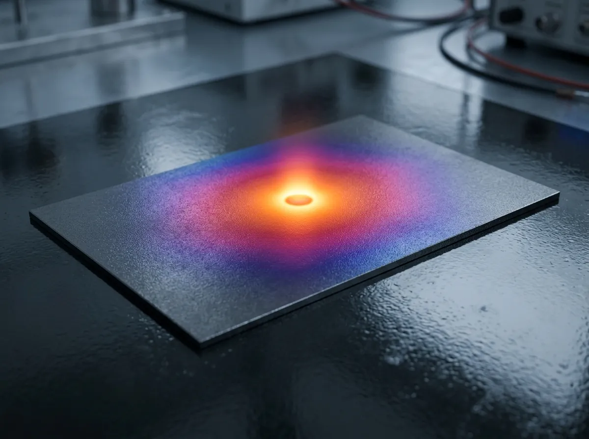
An anisotropic sheet is a lateral highway and a vertical fence: nearly all the heat that enters the graphite moves sideways to the large-area chassis contact.
Natural or Synthetic Graphite: Pick the Material Family First
The biggest fork in a graphite spreader specification is not the grade — it is the material family. "Natural" flexible graphite is compressed from mined graphite flakes; "synthetic" sheet (often called PGS or pyrolytic graphite sheet, and related to annealed pyrolytic graphite) is grown from polymer films at high temperature. They overlap in name but behave differently in the three dimensions that matter to a thin-device design.
Natural flexible graphite is thicker, tougher and cheaper. NeoGraf, a leading flexible-graphite producer, lists natural grades at 350–600 W/m·K in-plane with thicknesses up to about 0.9 mm, versus synthetic grades at 1,350–1,600 W/m·K at 0.017–0.050 mm — the eGraf SpreaderShield portfolio page is a good reference for both families side by side. Natural sheet tolerates handling, survives repeated flexing and low temperatures well, and is often used where the sheet doubles as a structural gasket or a thicker heat spreader behind large panels. Its cost advantage makes it the default when the thickness budget allows.
Synthetic (PGS-type) sheet is the phone-grade material: thinner, more conductive, and more fragile. Panasonic's PGS line, one of the most widely used in handheld electronics, illustrates the family logic on a single product series page: a 10 µm synthetic film is rated around 1,900 W/m·K, while a 100 µm film drops to roughly 700 W/m·K — conductivity falls as thickness rises, because the polymer-derived crystal alignment is best in the thinnest films. Synthetic sheet is brittle across its face and sheds flakes when creased, which is why virtually every phone-grade part ships laminated between PET and adhesive layers (the Panasonic EYG-A construction is PGS + PET + adhesive tape in one laminate).
The material family decision therefore cascades into thickness, cost and laminate construction simultaneously:
| Decision axis | Natural flexible graphite | Synthetic / PGS sheet |
|---|---|---|
| In-plane conductivity | 240–600 W/m·K | 700–1,900 W/m·K |
| Typical thickness | 0.13–0.9 mm | 0.012–0.10 mm |
| Handling & flex | Tough, survives creasing | Brittle — needs PET lamination |
| Temperature range | Very wide (cryogenic to ~300 °C) | Wide; laminate limits to ~150 °C |
| Typical use in thin devices | Panel backing, larger spreads, gaskets | Phones, tablets, SSD labels, tight z-stacks |
| Relative cost | Lower | Higher per area, offset by thinner stack |
In our own TIR series the split mirrors this exactly: the natural-grade TIR600 is specified at 240 W/m·K in-plane across 0.127–0.508 mm, while the synthetic-grade TIR300 line runs 1,200–1,700 W/m·K at 0.012–0.040 mm (the ultra-thin TIR312–TIR340 grades) with a -40 to 400 °C operating range for the bare film — the two families sit at opposite ends of the thickness-versus-conductivity trade. A quick browse of our TIR thermal graphite sheet range shows how each grade lines up against the other.
Thickness, Lamination and Adhesive: Engineering the Laminate
A raw graphite sheet is rarely the part that lands on your assembly line. What lands is a laminate: graphite core, pressure-sensitive adhesive (PSA) on one or both faces, a PET or polyimide carrier where the graphite is too fragile to handle alone, and a release liner that the pick-and-place or manual operator peels before assembly. Each layer is a design decision, not a packaging afterthought.
Thickness budget. Every tenth of a millimeter counts inside a phone. Synthetic cores are available down to ~0.012 mm and natural cores up to nearly a millimeter, and the choice interacts with what else occupies the same z-stack — shield can height, battery swell clearance, display driver routing. Because graphite carries heat in-plane, a thinner core with higher X-Y conductivity can outperform a thicker, lower-conductivity one: spreading resistance is governed by the cross-section area (thickness × width) and the conductivity together, so PGS's high λ at 25 µm often beats natural graphite at 200 µm in the same envelope. Model it; do not assume thicker is better.
Lamination and handling. Boyd, which builds encapsulated graphite structures from annealed pyrolytic graphite, is blunt about why containment matters: graphite is brittle and flaky, and loose flakes inside a device are a contamination and short-circuit risk — its heat spreader page describes encapsulation precisely to keep graphite particles from becoming foreign-object debris. For thin consumer devices the practical equivalent is PET lamination: the carrier stops edge flaking, gives the sheet tear resistance during handling, and can provide electrical insulation on the side facing live circuitry. If your graphite faces a battery or an exposed trace, specify which side is conductive and which is insulated — an uninsulated sheet touching a live pad is a field-failure report waiting to happen.
Adhesive. The PSA layer is simultaneously the thermal interface and the mechanical bond, and it is usually the thermally weakest link in the stack. Three checks matter: peel strength (the sheet must stay down through thermal cycling without lifting at edges), thermal resistance of the adhesive itself (thick, poorly-filled acrylics add real resistance; some suppliers offer thermally enhanced PSA), and temperature rating — standard acrylic softens or degrades well below the graphite's own 400 °C capability, and Panasonic's laminated PGS grades are derated to 150 °C for exactly this reason. Finally, specify die-cut geometry and registration tolerance with your part supplier: a graphite sheet is die-cut or kiss-cut into intricate shapes (with release-liner tabs for assembly), and dimensional tolerance on those features is where quality programs win or lose.
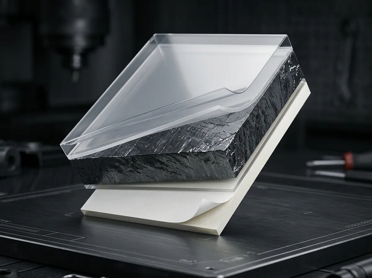
A phone-grade graphite part is a laminate: carrier film, graphite core, adhesive faces and release liner — each layer with its own thermal and mechanical job.
Graphite Sheet vs Vapor Chamber vs Heat Pipe vs Thermal Pad
Graphite sheets are not the only answer to thin-device heat, and specifying one without checking the neighbors is how teams end up with a 40 µm film trying to do a vapor chamber's job. The decision is about where the thermal bottleneck sits. Celsia's vapor chamber vs heat pipe guide frames it as three questions: how concentrated is the heat source, how far must the heat move, and how much resistance can the system tolerate. Graphite answers a narrower version of the same questions.
| Technology | Best when | Typical thin-device use | Watch out for |
|---|---|---|---|
| Graphite heat spreader sheet | Heat must spread from a point source across a large, thin area; z-height is minimal; no discrete fluid parts | Phones, tablets, SSD labels, panel backing, VR | Anisotropy: nearly useless through-thickness; fragile un-laminated |
| Thermal pad | A gap must be bridged through the z-axis with compression (chip to shield can, chip to spreader) | Interface between SoC and the graphite sheet or can | Pads fill gaps but do not spread heat far sideways |
| Heat pipe | Heat must be transported point-to-point over a longer distance to a remote sink | Laptop hinge-to-keyboard rails, tablets | Round pipes are thick; flattened pipes spread only locally |
| Vapor chamber | High, concentrated flux must spread across a broad plane before reaching fins/case | Gaming phones, high-end tablets, thin laptops | Can't match film thinness; cost and supply chain complexity |
The sequence that resolves most designs: use a thermal pad to get heat from the die into whatever spreads it; use a graphite sheet when that spreader must be a thin flexible plane over a wide area; escalate to a vapor chamber when the flux is so concentrated that even graphite's spreading resistance pushes the junction over budget; and reach for a heat pipe only when the heat has to travel tens of millimeters to a dedicated sink. In phones the mainstream answer is graphite over and around the SoC/shield stack with pads at the chip interfaces — a GPU thermal pad selection guide from the same cluster covers the pad side of that pairing in depth.
The graphite-versus-pad confusion deserves one explicit note: pads and graphite solve perpendicular problems. A pad is a z-axis material — you compress it between two surfaces to fill an air gap. A graphite sheet is an x-y material — you lay it flat to spread heat sideways. The "graphite thermal pad" phrasing you sometimes see on distributor sites usually refers to a thin graphite sheet with adhesive, not a compressible pad; when the spec calls for gap filling, buy a pad, and when it calls for lateral spreading, buy a sheet. And when the thermal path mixes both, that is normal — the sheet sits on top, pads underneath at each hotspot.
Where Thin Graphite Earns Its Keep: Phone, Tablet, SSD, VR
Once the selection logic is clear, the placements write themselves:
- Smartphones. The classic layout is a synthetic graphite sheet over the SoC and PMIC area, running under the shield can or across the midframe, with thin pads bridging chip-to-sheet. Sheets also back the battery (where a large lithium cell is a huge heat-sinking area), line the back cover above the wireless charging coil, and dress the display driver region behind the OLED. The TIR300 application list — mobile phones, handheld devices, notebooks, LCD/LED TVs and projectors — reflects how standard this usage has become.
- Laptops and tablets. Graphite appears behind the panel to pull backlight-driver heat to the edges, over the SSD and Wi-Fi module on the mainboard, and in the keyboard deck area. Where a thin heat pipe still handles CPU-to-rail transport, graphite fills the wide, low-flux areas around it.
- M.2 SSDs. The controller and NAND stack generate concentrated heat under a graphene or graphite label that doubles as the top thermal spreader inside the drive's limited envelope. A thin graphite sheet here reduces controller hotspot temperature more efficiently than a thicker pad of modest conductivity, which is why "thermal pad for SSD" and "graphite SSD label" describe two different layers in the same drive.
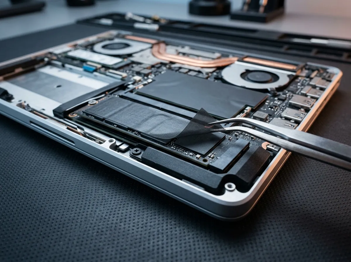
Inside an M.2 drive's thin envelope, a graphite label spreads controller and NAND heat across the whole drive surface — a job no pad can do.
- VR and wearables. Optics and display drivers sit close to the face, and the front housing is the only large sink — graphite sheets route SoC and driver heat to that housing while keeping the lens region cool, and the flexible sheet conforms to curved frames that a rigid spreader cannot follow.
In every case the golden rule from the anisotropy section applies: orient the sheet so the heat enters its plane, not its thickness. A sheet standing on edge between a chip and a cover transfers almost nothing; a sheet laid flat with a pad at the die is doing its job.
EMI and Grounding: Graphite Is Not an Absorber
Because graphite is carbon, a graphite sheet is electrically conductive, and that fact cuts both ways. It is why PGS-type sheets are sometimes specified for field suppression — Panasonic explicitly rates its PGS materials, on the product series page linked above, as ideal for electrical and magnetic field suppression up to 1,000 MHz — and it is why uninsulated sheets must never be allowed to contact live traces without intent. Insulated laminates (PET on the circuit side) exist precisely to decouple the thermal job from the electrical one.
The common misread is to treat a graphite sheet as an EMI absorber. A sheet can act as a shield or a ground/reflection plane — conductive surfaces redirect electric fields — but it does not provide the magnetic-loss absorption of a dedicated absorber material. When your noise problem is magnetic coupling from a switching regulator or a digital bus, the right addition is a magnetic-loss absorber, not more graphite. When the goal is a quiet ground reference or a reflective barrier, the graphite's electrical path, contact points and grounding need to be designed deliberately, not assumed. A thermal EMI absorber materials guide on this blog covers the pairing of conductive and absorptive layers inside shielded assemblies.
The specification language that keeps teams out of trouble: state whether each face of the graphite part must be electrically conductive or insulating, state where the sheet is allowed to contact grounded metal, and add an absorber separately if the test data shows magnetic noise. If the requirement is silent on EMI, the sheet will ship conductive by default — because it is.
What to Demand From a Graphite-Sheet Supplier
A graphite spreader is a material purchase with datasheet physics, but it becomes a quality problem when the supplier's numbers do not survive the transition to your line. Demand evidence on each of these before you commit a part number:
| Evidence to demand | Why it matters | What to check |
|---|---|---|
| In-plane conductivity with test method | X-Y W/m·K varies with measurement technique and temperature | Laser-flash or vendor method stated; value at room and operating temperature |
| Through-plane value and thermal impedance | Confirms the sheet is not being sold as a z-axis filler | Impedance per ASTM D5470 with pressure and thickness conditions stated |
| Thickness tolerance | ±10% on a 0.025 mm core is ±2.5 µm — significant against a tight z-budget | Confirm tolerance band and measurement standard (e.g., ASTM D751) |
| Adhesive peel strength and temperature rating | The PSA, not the graphite, usually fails first | Peel force, max continuous temperature, aging behavior |
| Insulation / conductivity of each face | Prevents field failures from graphite touching live circuitry | Explicit electrical spec per face; insulated versions documented |
| Flammability and compliance | Consumer electronics certification gates | UL94 rating at your thickness, RoHS/REACH status |
| Outgassing (for sealed optics/VR) | Volatiles fog lenses and contaminate sealed modules | Total mass loss / collected volatile condensables data if applicable |
| Die-cut tolerance and lot consistency | Registration and dimensional drift break automated assembly | Die-cut feature tolerance, CoA per lot, process control (IATF/ISO) |
Then validate on your own hardware. A short coupon test — your real stack, your adhesive, your ambient — with a thermocouple on the hotspot will separate the datasheet grade from the working part faster than any spreadsheet comparison. Sample the sheet through the exact construction you plan to buy (bare vs PET-laminated vs PSA on both sides changes the thermal path), measure before and after aging, and confirm the die-cut shape against your actual carrier.
A Five-Point Checklist Before You Write the Spec
- Draw the heat path. Identify the hotspot, the large-area sink (chassis, shield can, battery), and every interface between them. Mark which interfaces need z-axis gap filling (pads) and which need lateral spreading (sheets).
- Fix the material family. Natural flexible graphite for thicker, tougher, lower-cost spreads; synthetic/PGS sheet when the z-budget demands under ~0.1 mm or the conductivity target exceeds ~600 W/m·K.
- Engineer the laminate. Specify core thickness and tolerance, carrier and insulation on each face, PSA type with peel and temperature data, and die-cut geometry with registration tolerance.
- Check the technology boundary. Confirm a sheet is actually the right answer — escalate to a vapor chamber if spreading resistance dominates at high flux, to a heat pipe if transport distance is long.
- Demand the data. In-plane and through-plane values with methods, ASTM D5470 impedance at your conditions, UL94, RoHS/REACH, peel and tolerance evidence, and a coupon validation on your own assembly.
Getting the sheet right on paper is the cheap half; the expensive half is discovering at prototype that the graphite flakes at the die-cut edge, or the adhesive lifts after thermal cycling, or the 1,700 W/m·K number was measured at 25 °C on a film that never sees room temperature in your device. ZIITEK's TIR series spans both material families, and the thermal engineering team works through this exact checklist on consumer-electronics programs — if you want a second pair of eyes on your stack or samples for your own coupon test, send your thermal budget and envelope to our engineers and we will take it from there.