Thermally Conductive EMI Absorbing Materials: Selection Guide for 5G, RF and Optical Modules
Thermal conductive + EMI absorbing materials solve board-level heat and noise with one pad. Learn how they work, the specs that matter, and how to choose.
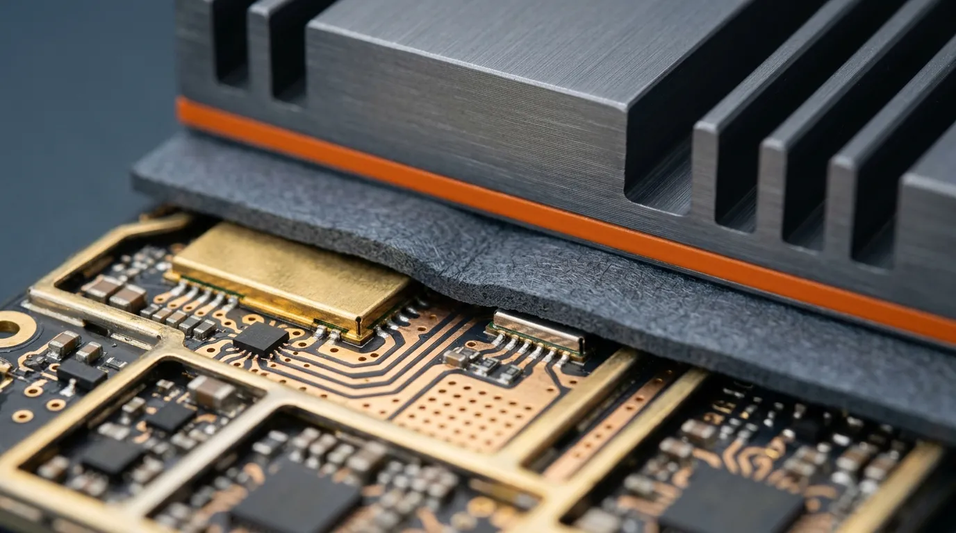
Modern high-speed electronics rarely face thermal and EMI challenges separately. Power-hungry processors, RF front ends, and high-speed optical modules generate heat while operating in increasingly dense electromagnetic environments. Traditionally, thermal pads, EMI shields, and absorber sheets have been used as separate components.
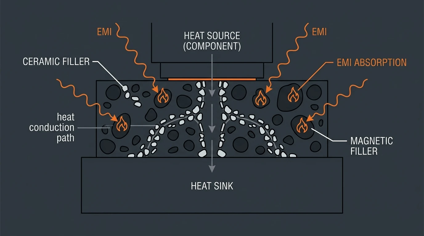
Thermally conductive EMI absorbing materials combine these functions in a single compliant interface. They provide a thermal path to the heat sink while attenuating electromagnetic energy within the target frequency range, helping engineers address thermal management and EMI suppression without adding another discrete component. Soft-magnetic filler particles give it a magnetic loss mechanism that turns noise into heat, and the same silicone matrix conducts that heat into a heat sink through its ceramic filler network. For 5G radios, optical modules, and other dense RF boards, this two-in-one material class is becoming an increasingly attractive solution for applications where both thermal management and EMI suppression are required.
If your board failed a radiated-emission test last week, or a shield can exhibits resonance around 2.4 GHz, or the DSP on your optical module is throttling — this guide covers what these materials are, which specs actually decide the outcome, and a three-step method for picking the right one.
Why One Material for Heat and Noise?
High-speed boards stopped being either hot or noisy a long time ago — they are usually both. A 5G radio front end burns power in the PA stage and switches at frequencies that couple straight into nearby traces. A 400G optical module runs a hot DSP beside SerDes lanes at 25 Gb/s and up, where every edge transition radiates. A Wi-Fi router packs four radios, a CPU, and a switch into a plastic box that resonates at the exact bands it transmits on.
The classic fix uses two or three parts: a thermal pad to move heat, a metal shield can or gasket to contain emissions, and sometimes an absorber sheet glued inside the can to kill cavity resonance. That works, but each part adds cost, assembly steps, height, and a new tolerance stack. A shield can also creates its own problems — a metal box around a noisy source can resonate and re-radiate if it is not designed carefully, and it blocks access for rework.
A thermal conductive EMI absorber collapses this stack into one part: it sits between the heat source and the heat sink like a normal thermal pad, and its absorbing action damps the noise at the source. One part, two functions, and fewer components in the mechanical stack-up. That is the trade-off this guide walks through, with real numbers instead of marketing language — the full series overview lives on our thermal conductive + EMI absorbing materials hub.
What Are Thermal Conductive EMI Absorbing Materials?
A thermally conductive EMI absorber is a composite sheet built from three ingredients:
- A silicone matrix that stays soft and conforms to uneven gaps, exactly like a conventional thermal pad.
- A ceramic filler (alumina, boron nitride, and similar) that creates a low-resistance heat path through the pad — this is what gives the material its W/mK rating.
- A soft-magnetic filler (ferrite-type particles) that responds to magnetic fields. When an electromagnetic wave interacts with the magnetic filler, part of its electromagnetic energy is dissipated through frequency-dependent magnetic loss mechanisms and converted into heat — this is the absorption mechanism, often called magnetic loss.
The two filler systems share the same sheet, which is why the material can be both a thermal interface material and a noise suppressor at once. The absorbed energy becomes heat, and the pad's own thermal path carries that heat into the heat sink — the two functions reinforce instead of fighting each other.
Two things matter in how the absorption is specified. First, attenuation: how many dB of the incident wave the pad removes at a given frequency, usually plotted as a curve. Second, the frequency band itself — absorbers are tuned, not broadband magic. A pad optimized for 10 MHz may provide little attenuation at 10 GHz. Industry explainers on how EMI absorbers work describe the same physics: mixtures of ceramic and iron, nickel, or zinc oxides that convert RF energy into heat. Published research on hybrid thermal/EMI absorber materials, such as this IEEE characterization study, confirms the practical trade-offs between heat conduction and absorption in a single layer.
Formats follow the application: thin sheets from about 0.03 mm up to 2.0 mm, with or without adhesive, and die-cut shapes for automated assembly. Because the material is silicone-based, it behaves like the thermal pads your line already handles — same compression, same placement tooling.
If you are new to the pad side of the equation, our guide to what a thermal pad is covers gap-filling basics and hardness before you mix in the absorbing requirement.
Absorber vs. Shield: Which Mechanism Does Your Board Need?
"EMI shielding material" and "EMI absorbing material" get used interchangeably in product listings, but they solve different problems, and mixing them up is the most common selection error in this space.
| Mechanism | How it works | What happens to the wave | Best for | Typical limit |
|---|---|---|---|---|
| Shielding (metal foil, can, gasket) | Conductive surface reflects or redirects the wave | Wave bounces back into the enclosure | Containing far-field radiation and meeting radiated-emission limits | Reflected energy can re-couple and ring |
| Absorption (magnetic-loss pad) | Soft-magnetic filler dissipates wave energy as heat | Wave is removed, not bounced | Cavity resonance, surface currents, near-field noise, ringing inside cans | Absorbs only in its tuned band; adds a thermal path you must size |
| Combined thermal + absorber pad | Absorbs noise and conducts heat in one part | Wave removed, heat moved to sink | Hot chips in noisy boards (5G, optical, RF) | Thicker than a plain pad at the same band |
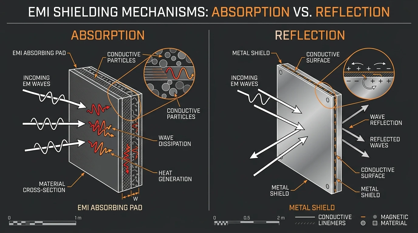
Metal is the traditional answer, and it works — research on flexible composites with high thermal conductivity and EMI shielding is still chasing foil-like performance in polymer form. But foils and cans reflect: the energy stays inside the system and can re-radiate through seams, apertures, or cable exits. That is why a shield can sometimes makes emissions worse at a specific frequency — the can becomes a resonant cavity.
An absorber, by contrast, removes the energy. When the problem is a resonance in a shield can, a ground-plane bounce, or unintended coupling through the heat sink or other conductive structures, a thin absorber sheet inside the enclosure is often the fastest fix. In practice, mature designs use both: a can for containment, an absorber inside it to kill the resonance — and where the noisy component also runs hot, a combined thermal + absorber pad replaces the plain pad underneath.
The regulatory pressure behind all of this is real: radiated-emission limits such as FCC Part 15 for unintentional radiators are what force most of these redesigns in the first place.
The Specs That Matter: Frequency, Permeability, and Thickness
Three numbers decide whether a thermal conductive EMI absorber actually fixes your board. Most datasheets bury two of them.
Initial permeability (µi) indicates the material's magnetic response under specified low-field test conditions. The test frequency should always be checked on the datasheet because it can vary by material and supplier. Higher µi means stronger low-frequency absorption — but it usually means a denser, heavier pad and a harder trade against thermal conductivity. Typical commercial absorbers sit in the µi 30–200 range. If a datasheet does not state µi, ask for it; it is the first number an applications engineer reaches for.
Frequency band. The absorption band is tuned by filler composition, particle size, thickness, and permeability together. Absorption performance is strongly dependent on thickness because thickness interacts with the material's frequency-dependent permeability, permittivity, and impedance matching. Therefore, the supplier's frequency–thickness performance data is more reliable than a simple rule that thicker always means lower-frequency absorption. — but the rule is relative, not absolute, because thickness and permeability interact. That interaction is exactly why the datasheet's frequency–thickness map matters more than any blanket rule. It is also why "absorber" is never a complete spec without a band — and why band matching is step one of selection, covered next.
Thermal performance. W/mK tells you how fast heat moves through the pad; thermal impedance (°C·in²/W) tells you the actual resistance at your working pressure, which is the number that matters in a real stack. For combined thermal + absorber pads, 1.5–4.0 W/mK covers most board-level needs — enough to cool a DSP or PA without turning the pad into a slab. Two electrical specs matter too, mostly at mmWave: dielectric constant and loss tangent tell you how the pad affects nearby signal traces, which is why high-frequency designs specify them explicitly. How to read W/mK properly (and why impedance beats conductivity in real designs) is explained in our thermal conductivity / W/mK primer.
One manufacturer's absorber line shows the typical band structure. As a representative example, the ZIITEK TIR900 series splits the spectrum into three classes:
| Series class | Absorption band | Initial permeability (µi @ 1 MHz) | Typical thickness |
|---|---|---|---|
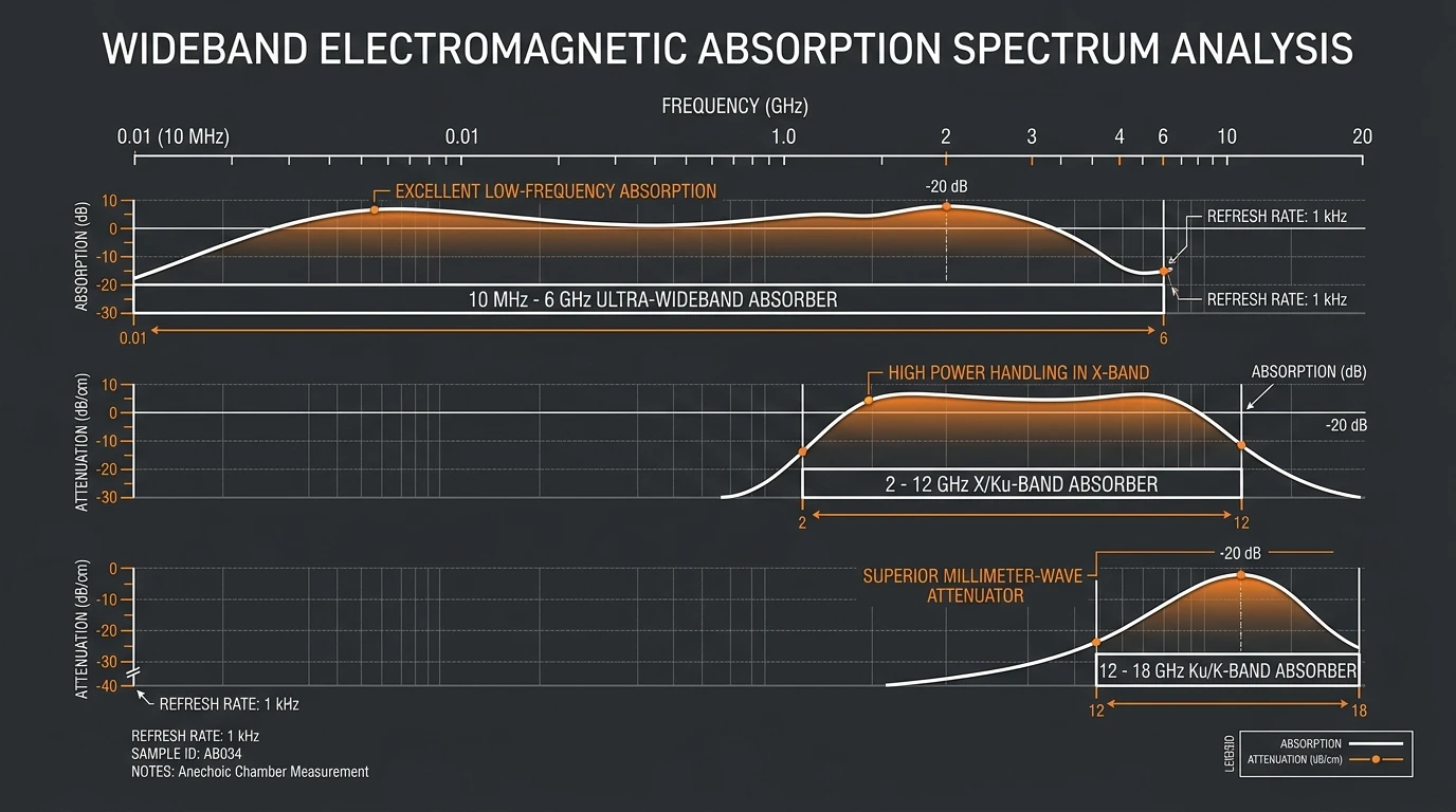
| TIR930-A ~ TIR9200-A | 10 MHz – 6 GHz | 30–200 | 0.03–0.50 mm |
| TIR-GC | 2 GHz – 12 GHz | — | 0.50–2.00 mm |
| TIR-HK | 12 GHz – 18 GHz | — | 0.50–2.00 mm |
The same physics appears across the industry — research on filler composites shows that both thermal conduction and EMI performance in these materials are governed by the same percolated filler network, which is why pushing one property usually moves the other.
How to Choose: A Three-Step Selection Framework
Instead of comparing datasheets line by line, work the problem backward from three questions.
Step 1 — Identify the noise: which frequencies, and where? Run a pre-compliance scan or review the failing spectrum. Sub-6 GHz noise (Wi-Fi at 2.4/5 GHz, 5G NR bands, switching power supplies) wants the 10 MHz–6 GHz material class. mmWave applications such as 28/39 GHz 5G require absorber grades specifically characterized for those frequencies, while applications in the 2–18 GHz range can be matched to the corresponding absorber class. If the noise is broadband, cover the dominant failing band first — an absorber tuned there will usually help the rest. If you are not sure whether the problem is radiation or conduction, the absorber-vs-shield decision above is the place to start.
Step 2 — Size the heat: how much W/mK do you actually need? Work from the thermal budget: die temperature target, dissipated power, heat sink capacity. Combined pads in the 1.5–4.0 W/mK range (for example, ZIITEK's TIF900 family spans exactly that range, with 1.5 to 4.0 W/mK across its grades) handle most module and board-level loads. Check thermal impedance at your real mounting pressure, not just the headline conductivity.
Step 3 — Fit the space: thickness, hardness, and shape. Thickness follows the datasheet's frequency–thickness map, not a blanket rule. In the TIR900 example above, the low-frequency class (10 MHz–6 GHz) achieves its band with high-permeability filler (µi 30–200) in thin 0.03–0.50 mm sheets, while the 2–18 GHz classes use 0.50–2.00 mm — so low-frequency absorption does not automatically call for a thick pad. Thin sheets suit tight stacks and small gaps; the 0.5–2.0 mm classes fill larger gaps and can also absorb at higher bands. Hardness (Shore 00) controls how much pressure the pad needs to conform, and whether it will crush components. Finally, plan the geometry: die-cut pads with tight tolerances assemble faster than hand-trimmed sheets, and peel-and-place adhesive layers remove one more process step. If your other option is a dispensable material, see how gap fillers compare with pads and phase-change materials before committing.
Three mistakes show up in almost every failed application:
- Choosing by W/mK alone. The best-conducting pad in the world does nothing if it absorbs in the wrong band.
- Buying a microwave absorber when the problem is thermal, or vice versa. One property does not imply the other.
- Underestimating thickness tolerance. A pad that absorbs at 1 GHz at 1.0 mm may shift out of band at 0.8 mm if the stack compresses it more than the datasheet assumed.
Applications: 5G Radios and Optical Modules
The two application families in this cluster's name are where the two-in-one class earns its keep.
5G radios and base stations. The PA and front-end stages run hot and switch at sub-6 GHz and mmWave frequencies at the same time. A combined pad between the module and the heat sink removes the heat and damps the board-level noise in one assembly step — one fewer part inside a sealed radio, one fewer tolerance stack, one fewer thing to fail in the field. The same logic applies to small cells and customer-premises equipment: plastic enclosures do not shield, so absorption is often the only practical tool for board-level control.
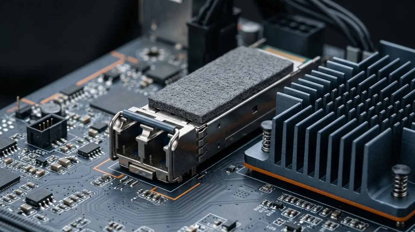
Optical modules and transceivers. A 400G or 800G module concentrates a hot DSP and very fast SerDes lanes in a small, shielded package. The classic failure pattern is a module that meets its optical specs but fails radiated emission or crosstalk limits because the high-speed edges couple into the cage or the host board. A thin thermal conductive EMI absorber between the module and its heat sink both extracts the DSP heat and damps the edge noise — and at 0.03–0.5 mm it fits inside the existing mechanical envelope. We covered the thermal side of this exact problem in our AI optical module thermal management case study.
Beyond those two: Wi-Fi routers and mesh nodes (2.4/5 GHz resonance in plastic enclosures), automotive electronics (ADAS and infotainment under vibration and temperature cycling), and satellite communication terminals in the 12–18 GHz band all use the same frequency-first selection logic. 5G thermal management in the field is rarely one big problem — it is a dozen small hot-and-noisy spots, each solved by the right pad class.
Compliance and Reliability: UL 94, RoHS, and Beyond
B2B buyers cannot take a pad's claims at face value — the certification stack is part of the spec.
- Flammability. UL 94 V-0 is a material flammability classification based on specified vertical-burning test criteria, including afterflame time, afterglow, and flaming drips. Always verify the rating for the specific material and thickness being used, and this rating is a hard requirement in many telecom, automotive, and consumer designs. Check the yellow card, not just the datasheet line.
- Substance restrictions. RoHS and REACH compliance is table stakes in EU-bound and most global products; halogen-free and lead-free formulations matter for safety and recycling requirements.
- Working temperature range. A typical silicone-based pad runs from about −45 °C to 200 °C, which covers most electronics; low-outgassing (low TML) grades exist for sealed optical assemblies where volatile residues would fog lenses or coat contacts.
- Shelf life and handling. Absorbers store like thermal pads — dark, cool, dry — and most carry a multi-year shelf life from the manufacturer's date code.
The safety standards that reference these ratings, such as IEC 62368-1 for audio/video and ICT equipment, are part of why a UL-recognized material with documented test reports moves through customer qualification faster than an unrated equivalent. Ask for the test reports; a supplier with the certificates will not hesitate to share them.
What to Ask a Supplier Before You Buy
Five questions will separate a supplier who understands the material from one who is reselling a spec sheet:
- "What is the absorption band, and can I see attenuation data across it?" A curve is worth a thousand "broadband" claims.
- "What is the initial permeability (µi), and how does the band shift with thickness?" You need both numbers to match your failing frequencies.
- "What W/mK and thermal impedance do I get at my mounting pressure?" Impedance at real pressure beats headline conductivity every time.
- "Can I have the UL 94, RoHS, and REACH documentation up front?" Compliance should be downloadable, not promised.
- "Do you die-cut to tolerance, and what is the lead time?" Production-ready shapes with documented tolerances save an assembly step and a rework loop.
Then ask for samples and test them in your own failing board — the fastest qualification is the one where the measurement happens on your spectrum analyzer, not in a marketing slide. ZIITEK supplies thermal pads, absorber sheets, and combined thermal + absorber materials (TIR900 and TIF900 series) with datasheets and samples available through the thermal pad product range — or contact the engineering team for band matching against your failing spectrum.