Understanding Thermal Conductivity (W/mK) in TIM
A TIM's W/mK measures bulk conductivity, not real cooling. Learn what W/mK means, why the datasheet number misleads, and what predicts junction temperature.
Two thermal interface materials sit on your desk. One datasheet reads 8 W/mK, the other 3 W/mK. The choice looks obvious — until you assemble both and the “slower” material runs your component cooler. If you have ever stared at a spec sheet wondering why the bigger conductivity number didn’t win, you are asking exactly the right question.
Thermal conductivity, measured in watts per meter-kelvin (W/mK), is the single most-quoted number on any thermal interface material (TIM) datasheet. It is also the most misunderstood. W/mK tells you something real and useful — but on its own it does not predict how cool your part will run. This guide explains what W/mK actually measures, why the bulk number and real-world performance diverge, and which figure you should specify a TIM on instead. For the full material-selection workflow, see our Thermal Interface Materials: The Complete Selection Guide.
What thermal conductivity (W/mK) actually means
Thermal conductivity (symbol k, sometimes λ or κ) is a material’s intrinsic ability to conduct heat. It is defined by Fourier’s law of conduction, which in its simplest one-dimensional form states that heat flux is proportional to the temperature gradient:
q = −k · ∇T
where q is heat flux (W/m²), ∇T is the temperature gradient (K/m), and k is the constant of proportionality — the thermal conductivity (Wikipedia: thermal conductivity and resistivity).
The unit W/mK (watts per meter-kelvin) falls straight out of that equation. In plain language: a material with a conductivity of 1 W/mK conducts one watt of heat through a one-meter-thick slab, across each square meter of area, for every one-kelvin temperature difference across it. Higher k means heat moves through the material more readily.
The critical word is intrinsic. Thermal conductivity is a bulk material property, independent of geometry. It describes the material itself — not the part you build from it, and not the interface where two parts meet. A block of aluminum and an aluminum foil have the same conductivity; they perform very differently in an assembly. Hold on to that distinction — it is the whole story of this article.
For reference, here is where common materials land:
| Material | Approx. thermal conductivity (W/mK) |
|---|---|
| Still air (the enemy) | ~0.026 |
| Unfilled silicone/polymer | ~0.1 |
| Modern filled TIM (paste/pad) | ~1 – 18 |
| Alumina filler (Al₂O₃) | ~30 |
| Aluminum | ~200 |
| Copper | ~400 |
| Liquid-metal TIM | ~35 – 58 |
Unfilled polymers conduct heat poorly — around 0.1 W/mK — which is why every modern TIM is a composite loaded with conductive filler particles to push conductivity into the useful range (Electronics Cooling: thermal interface materials).
Why a TIM needs a high W/mK in the first place
To understand why the number matters, look at the problem a TIM solves. When you bolt a heat-generating die, package, or battery cell against a heat sink, the two surfaces look flat but are microscopically rough. Under magnification they touch only at a few high points; the rest of the “contact” is a field of tiny air gaps.
Air is a superb insulator — about 0.026 W/mK, roughly 40 times worse than even a modest 1 W/mK TIM, and some 700 times worse than a high-end 18 W/mK gap pad. Left alone, those trapped air voids would throttle heat transfer across the joint. The job of a thermal interface material is to flow into that microscopic terrain, displace the air, and replace it with something far more conductive.
That is why formulators load a soft silicone or non-silicone matrix with conductive fillers — alumina, boron nitride, aluminum, zinc oxide, and others. More filler generally means higher W/mK. But filler loading is a balancing act: pack in too much and the material gets stiff, harder to compress, and thicker at the joint — which, as the next sections show, can erase the conductivity gain you paid for.
W/mK across the TIM families: what “high” really means
Different TIM formats occupy very different conductivity bands. The table below shows ZIITEK’s product ranges, which track the industry at large and give you a realistic sense of what each format delivers:
| TIM format | ZIITEK series | Typical W/mK |
|---|---|---|
| Thermal grease / paste | TIG®780 | 1.0 – 5.2 |
| Thermal gel / dispensable gap filler | TIF® gel | 1.5 – 9.0 |
| Silicone gap pad | TIF® | 1.25 – 18 |
| Phase change material (PCM) | TIC®800 | 0.95 – 9.6 |
| Carbon-fiber pad | TIR®700 | 9 – 35 |
| Non-silicone pad | Z-Paster®100 | 1.5 – 10 |
| Thermal insulating pad | TIS® | 1.0 – 1.6 |
| Thermal double-sided tape | TIA®600/800 | 0.8 – 1.6 |
| Liquid metal | Liquid Metal | 35 – 58 |
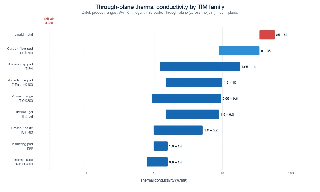
A few things jump out. Liquid metal towers over everything on paper. Carbon-fiber pads reach surprisingly high — but note a subtlety the datasheet may not headline: some materials are anisotropic, conducting far better in-plane (along the sheet) than through-plane (across the joint, which is the direction you actually care about).
Our own TIR®300 graphite sheet makes the point about as starkly as it can be made. It conducts at 1,700 W/mK in-plane and 5 W/mK through-plane — a 340× gap between two directions in the very same product. Read the headline number and it appears to outclass copper by four times over; put it across a bond line and it behaves like a low-single-digit material. That is not a defect: a graphite sheet’s job is usually to spread heat sideways to a larger surface, and 1,700 W/mK is precisely why you would specify one. The number only misleads when the direction goes unstated. Oriented carbon-fiber pads such as TIR®700 (9–35 W/mK) are the opposite case — the fibers are aligned to conduct through the pad, so the rating you are quoted is the one your joint gets. Same “high W/mK carbon material” shelf, entirely different physics. Always confirm which direction a W/mK figure refers to.
If you are still deciding between formats before you even reach conductivity numbers, our guide to thermal pad vs. thermal paste covers that fork.
Why bulk W/mK doesn’t predict real-world performance
Here is the crux. The W/mK on a datasheet is the material’s bulk conductivity, measured under controlled lab conditions. What you actually care about is how much the TIM lowers your junction temperature in a shipped assembly — and those two things can disagree.
Start with the physics of a real joint. The thermal resistance of a TIM layer is:
Rθ = t / (k · A) — units: K/W
where t is the bond line thickness (BLT), k is conductivity, and A is the contact area. Keep an eye on that area term; it is the difference between two numbers the industry constantly conflates, and we will come back to it. Two consequences follow immediately:
- Thickness matters as much as conductivity. Resistance scales with BLT. A material with double the W/mK but sitting at double the thickness gives you the same bulk resistance. Because W/mK carries no thickness information, the datasheet number alone cannot tell you the resistance of your joint.
- The joint has more resistance than the bulk. The TIM doesn’t fuse perfectly to the die and the heat sink; there is a thermal contact resistance at each face, driven by surface roughness, wetting quality, and how hard the joint is compressed.
This is why “effective” or “apparent” conductivity figures are so slippery. As Electronics Cooling puts it, an effective conductivity value “can be used to calculate the temperature difference across a TIM with full accuracy only at the thickness at which it was measured” — apply it at a different bond line and you introduce significant error (Electronics Cooling: calculations for thermal interface materials).
A worked example makes the trap concrete. Suppose you compare:
- Material A — a stiff gap pad rated 12 W/mK, but so highly loaded it won’t compress below a 150 µm bond line and wets the surfaces poorly (adding contact resistance).
- Material B — a conformable gel rated 6 W/mK that squeezes to a 50 µm bond line and wets both faces cleanly.
Work the bulk term for a 1 cm² joint. The step people skip is the unit conversion: W/mK is defined per meter, so convert before you divide — 12 W/mK = 0.12 W/cm·K, and 150 µm = 0.0150 cm.
- Material A: 0.0150 cm ÷ 0.12 W/cm·K ≈ 0.125 cm²·K/W of bulk area-specific resistance. Across a 1 cm² joint that is Rθ = 0.125 cm²·K/W ÷ 1 cm² ≈ 0.125 K/W — plus meaningful contact resistance from poor wetting.
- Material B: 0.0050 cm ÷ 0.06 W/cm·K ≈ 0.0833 cm²·K/W, i.e. Rθ ≈ 0.0833 K/W across the same 1 cm² — plus low contact resistance.
Sanity-check any such figure against reality before you trust it: real TIM joints land around 0.05–0.5 cm²·K/W. A result two orders of magnitude below that band isn’t a miracle material — it is a dropped unit conversion, and it is the most common arithmetic slip in TIM comparison. (Note also what the units are doing: divide by the area and you are in K/W, the resistance of your joint; leave the area out and you are in cm²·K/W, a figure any size of part can be compared on. The next section leans on that difference.)
The “half as conductive” material wins — its thinner, better-wetted joint beats the headline number. The datasheet said 12 versus 6; the assembly said the opposite. Bond line thickness and compression are so decisive here that they deserve their own treatment — see our thermal pad thickness & compression guide.
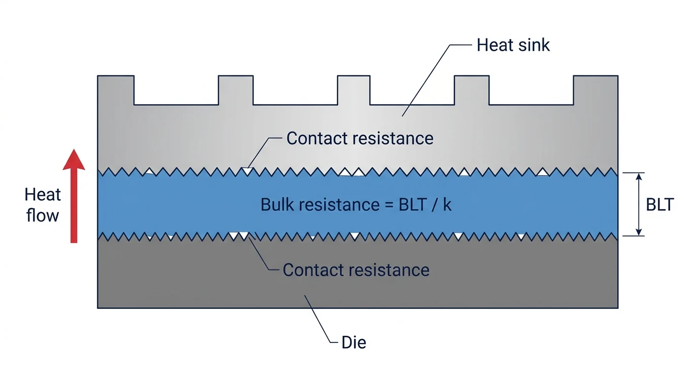
Thermal impedance and contact resistance: the numbers that actually matter
If W/mK is only half the story, what completes it? Thermal impedance — the metric that bundles everything a real joint contributes into one figure.
For a TIM between two surfaces, the impedance of the joint is:
θ_TIM = (BLT / k_TIM) + θ_c1 + θ_c2 — units: °C·cm²/W (K·cm²/W)
where the first term is the bulk contribution and θ_c1 and θ_c2 are the contact resistances at each face (Electronics Cooling: thermal interface materials — a brief review).
Watch the units, because this is where the two most-confused numbers in the field separate. Every term in that equation is already area-normalized — BLT ÷ k is metres over W/mK, which lands in m²·K/W, not K/W. That is exactly what makes θ an impedance: a per-unit-area figure you can compare across parts of any size. To get back to the thermal resistance of your joint, divide by the real contact area — Rθ = θ_TIM / A, in K/W — which is the same relationship as the Rθ = t/(k·A) we started from, just rearranged. Unlike bulk conductivity, impedance captures the bond line, the wetting, and the interface: it is a property of the joint, not just the material. (One more comparison trap: US datasheets often quote °C·in²/W rather than °C·cm²/W, and 1 °C·in²/W ≈ 6.45 K·cm²/W. Comparing the raw numbers without converting is the same class of error as the one in the worked example above.)
That is why datasheets for thin-bond products such as greases and phase change materials list thermal impedance at a stated pressure, not just W/mK — it is simply the more honest, more useful number for a designer. It is measured by the industry-standard ASTM D5470 test, which derives apparent conductivity by measuring impedance across several thicknesses and taking the slope, precisely so the interface resistance is separated out.
Two practical cautions come with impedance:
- Test-method variance. W/mK and impedance figures depend on the test rig, pressure, and reference method — and the spread is not small. D5470 itself reports a round-robin study in which calculated apparent thermal conductivity landed within ±18% of the mean across the participating laboratories (C-Therm: thermal impedance vs thermal conductivity). Two “5 W/mK” products from different suppliers are therefore not guaranteed to be equivalent, and neither are two labs measuring the same product. Treat the spec as an upper-bound indicator, not a promise.
- Direction. As noted earlier, confirm whether a conductivity figure is through-plane (the useful direction) or in-plane.
For a deeper walk through these terms and how they interrelate, see thermal resistance vs. thermal impedance explained.
How to actually use W/mK when specifying a TIM
W/mK is not useless — it is a filter, not a verdict. Here is a workflow that puts the number in its proper place:
- Shortlist by material class using W/mK. Use conductivity to rule material families in or out for your power density and gap. A 0.8 W/mK tape and a 35 W/mK carbon-fiber pad are not competing for the same job.
- **Compare finalists on thermal impedance at your conditions.** Once you are down to candidates, stop comparing W/mK and start comparing impedance at the pressure and bond line your design actually applies. This is where the real ranking emerges.
- Match the format to the gap and mechanics. A large or uneven gap wants a conformable gel or gap filler; a flat, high-clamp CPU lid wants a thin grease, PCM, or liquid metal. Conductivity only helps if the material can reach a thin, void-free bond in your geometry.
- Weigh reliability, not just day-one numbers. Greases can pump out or dry out over thermal cycles; PCMs re-flow; stiff, highly-filled pads exert mounting stress. The highest W/mK is a poor trade if performance degrades in the field.
- Consider electrical needs. If the TIM must also isolate voltage, dielectric strength constrains your choices — a pure high-conductivity metal-loaded material may be disqualified regardless of W/mK.
For the complete decision tree across all of these factors, follow our guide on how to choose a thermal interface material.
Common questions about W/mK, answered
Is 8.5 W/mK good for a TIM? For a gap pad or gel, 8.5 W/mK is genuinely high-performance; for a carbon-fiber pad or liquid metal it is mid-pack. “Good” only means something relative to the format and, more importantly, to the thermal impedance you achieve at your bond line. A well-wetted 5 W/mK material at 40 µm can beat a poorly-seated 8.5 W/mK one at 150 µm.
What is a good W/mK for thermal paste? Mainstream thermal greases land roughly between 1 and 5 W/mK; premium and metal-loaded pastes push higher. Above that band you are usually into liquid metal, which brings its own handling and compatibility constraints. What matters for a paste is a thin, complete, void-free bond — see how to apply thermal paste correctly.
Why can a thick, high-W/mK pad run hotter than a thin film of lower-W/mK paste? Because a joint’s impedance is bond line thickness divided by conductivity, plus the contact resistance at each face. The bulk term scales directly with thickness, and a thick pad often wets less completely than a thin, flowable paste. The paste’s thin, conforming bond can win despite a lower headline conductivity — exactly the trap this article exists to flag.
Higher or lower W/mK — which do I want? For a TIM you almost always want higher through-plane conductivity, all else equal. But “all else” — bond line, wetting, pressure, reliability, dielectric needs — is rarely equal, which is why you spec on impedance, not on W/mK alone.
The bottom line
Thermal conductivity in W/mK is the right place to start evaluating a thermal interface material and the wrong place to stop. It is a bulk material property that tells you the ceiling of what a formulation can do — but the number your component actually feels is thermal impedance, set by bond line thickness, contact resistance, wetting, and pressure. Read the datasheet W/mK as a shortlist filter, then compare finalists on impedance at your real operating conditions, and you will stop being surprised when the “slower” material runs cooler.
ZIITEK engineers TIMs across every format in the table above — grease, gel, gap pads, PCM, carbon-fiber, and non-silicone — from an IATF 16949:2016 and ISO 9001 certified operation, with UL Yellow Card E331100 (UL 94 V-0) listings and Guangdong’s Thermal Materials Engineering Technology Research Center behind the formulation work. If you are matching a material to a specific thermal budget, our complete thermal interface material selection guide walks the full decision — so you can spec with confidence on the number that counts.