What Are Vapor Chambers? TIM in the Stack
What a vapor chamber is, and where the thermal interface material sits in the stack: TIM1 at the die, TIM2 at the sink, flatness, bond line and pump-out.
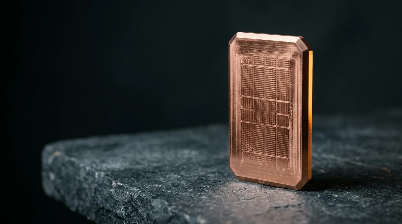
A vapor chamber is a sealed, evacuated plate that moves heat by boiling and condensing a working fluid, spreading it across two dimensions instead of one. Ask what a vapor chamber thermal interface material has to do and you reach the part most explanations skip: the chamber is only as good as the two thin layers above and below it.
That is the whole argument of this article. A 20 × 20 mm accelerator die dissipating 300 W produces 75 W/cm² at the contact face. The chamber can spread that heat across a plate with an effective conductivity tens of times that of solid copper and still lose most of the gain at a 60 µm grease layer nobody measured, or at a die corner where the chamber does not touch anything at all.
The Short Answer: Two Interfaces, Not One
Every vapor-chamber stack has a die-side interface and a sink-side interface, and they fail for different reasons. Which one you control depends on how the stack is built.
| Build | Die-side interface | Chamber's role | Sink-side interface |
|---|---|---|---|
| Bare-die chamber | TIM1 directly on the die: grease, phase-change film or liquid metal | the chamber is the heat-sink base | TIM2 to the fin stack or cold plate |
| Lid plus chamber | TIM1 from die to integrated heat spreader, often solder | bolted or clamped over the lid | TIM2 lid to chamber, then a second TIM2 from chamber to cold plate |
| Chamber as lid | solder die attach, no polymer TIM1 | the chamber is the lid | TIM2 from chamber to cold plate |
The builds differ in where the thin layers land, not in whether they exist. A solder die attach removes one polymer interface and adds a reflow step that can bow the plate. A bare-die chamber removes the lid and puts the polymer layer on the die itself, where the area is smallest and the heat flux highest. In a 1U tray the whole stack has a couple of centimeters of height to work with, which is one reason the spreader is a plate rather than a block.
The data-center and AI-server thermal material guides cover the neighboring topics — gap fillers, high-conductivity pads, liquid metal. This piece stays on the chamber and its interfaces.
What Are Vapor Chambers, and What They Are Not
A vapor chamber is a flat, sealed envelope with three internal parts: a wick lining the walls, a small charge of working fluid, and an open vapor space between them. Heat enters at the evaporator, which is the area over the die. The fluid boils, the vapor crosses the cavity almost instantly, condenses on the cooler face above the fins, and the wick returns the liquid by capillary action. Water is the usual fluid; acetone appears where the operating range is colder.
Two consequences follow from the geometry. First, spreading is two-dimensional: a heat pipe carries heat along its length, and a chamber distributes it across a plane, which is why it replaces the base of a heat sink rather than a length of heat pipe. Advanced Thermal Solutions reports effective conductivity above 10,000 W/m·K for a well-made chamber, against roughly 400 W/m·K for solid copper. Second, the device is a thin shell. The copper faces are a fraction of a millimeter thick, held apart by sintered posts or a stamped pattern, then brazed or welded and evacuated. That shell is why the mechanical rules later in this article matter as much as the thermal ones.
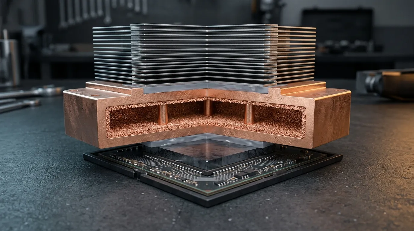
What a chamber is not. It is not a heat sink — it has almost no surface area to reject heat to air, so it still needs fins or a cold plate. It is not a thermal interface material, and it does not repair a bad joint underneath it. And it does not fix a stalled airflow path: a chamber spreads heat into a sink that must still be able to reject it.
The chamber's own limits are worth naming before the interfaces, because they set the ceiling. Each wick has a capillary limit: push enough power through a thin chamber and the evaporator dries out, the vapor space fills with superheated vapor, and the temperature climbs until the loop re-primes or the die throttles. Water-filled chambers cannot be stored or shipped below freezing without care, and a chamber run against gravity loses capacity compared with the same part run with gravity assist.
There is also a case for not using one. When the heat load is modest, the height budget is generous and the tooling cost matters more than the last few degrees, a heat pipe and a solid base will do the job — the chamber earns its price only when spreading, not transport, is the bottleneck.
Where the TIM Sits: TIM1, TIM2 and the Solder Joint
The naming is older than the packages. TIM1 is the layer between the die and whatever spreads heat off it. TIM2 is the layer between that spreader and the next level of hardware — a heat sink, a cold plate, a chassis wall. A build that stacks a lid and a chamber under one cold plate therefore has two TIM2 layers; the numbering counts levels above the die, not a fixed number of interfaces. The distinction that matters is still the same: TIM1 sees the highest heat flux and the smallest area, while TIM2 sees a larger area, a less uniform gap and the mounting load.
| Interface | What it couples | Options | What dominates |
|---|---|---|---|
| TIM1, bare die | die face to chamber base | grease, phase-change film, liquid metal, thin pad | bond line at the die edge, die bow, pump-out |
| Die attach | die to lid or chamber | gold-tin or tin-antimony solder | voiding at the die corners, CTE stress |
| TIM2 | chamber to fin stack or cold plate | grease, phase-change film, pad, graphite sheet | gap uniformity across a large face, clamp load |
| Structural bond | chamber to carrier or frame | epoxy or braze | flatness after cure, not before |
A vapor chamber thermal interface material choice is therefore not one decision. The same supplier may be right for TIM2 and wrong for TIM1, and a stack that uses solder at the die still has a polymer interface at the sink. The TIM stack for AI accelerators walks through the same layers from the package side.
Solder deserves one paragraph, because it changes the failure mode rather than removing the interface. A soldered die attach has no pump-out and no dry-out; what it has is voids, intermetallic growth and a stiffness mismatch that pushes stress into the die and the lid. A solder layer that is 90 percent wetted still fails if the voids sit at the corners, where the die is coolest during reflow and where the thermal path is longest.
Vapor Chamber Thermal Interface Material: Why 50 µm Beats a Better W/m·K
Interface resistance has three terms in series: the contact resistance into the material, the bulk resistance through it, and the contact resistance out of it. The bulk term is the only one a datasheet number describes, and it is written as bond-line thickness divided by conductivity. Keep it apart from the chamber's own benefit: the chamber earns its place by cutting spreading resistance, while the layer under it spends resistance in bulk and contact terms. Adding the two as if they were the same quantity is where stack budgets go wrong.
R_TIM = BLT / k_TIM + R_contact,1 + R_contact,2
That equation is area-specific — m²·K/W — so divide by the die area to reach the K/W figures below. Both the equation and the observation that contact resistance dominates as the layer gets thin are standard in the review literature on thermal interface materials. Put numbers on it for a 20 × 20 mm GPU or ASIC die — 400 mm², 4 × 10⁻⁴ m² — at 300 W:
| Interface | k (W/m·K) | Bond line | Bulk R (K/W) | ΔT at 300 W |
|---|---|---|---|---|
| Grease | 5 | 50 µm | 0.025 | 7.5 °C |
| Grease | 5 | 150 µm | 0.075 | 22.5 °C |
| Pad | 8 | 200 µm | 0.063 | 18.8 °C |
| Pad | 16 | 150 µm | 0.023 | 7.0 °C |
| Pad | 16 | 250 µm | 0.039 | 11.7 °C |
Two readings. Tripling the bond line of the same grease costs 15 °C at this power, which is more than most people expect from a layer they cannot see. And a 16 W/m·K pad at 150 µm lands at 7.0 °C — within half a degree of 5 W/m·K grease at 50 µm. Conductivity and thickness trade against each other almost linearly; you cannot buy your way out of a gap you have not measured. That parity is bulk only — a pad's two contact terms are usually larger and more pressure-sensitive than a grease's, so match bulk resistance first and then confirm contact resistance in your own stack.
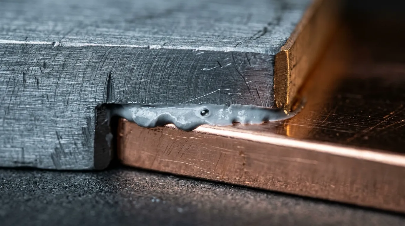
There is a second trap in that review: raising the filler loading raises conductivity and raises the bond line at the same pressure, because the material yields less easily. That is why a high-k grease can measure worse than a mid-k one in a real assembly. The correlation behind it was validated between 25 and 200 psi (about 0.17–1.4 MPa) in a review of TIM design characteristics, which covers most server clamping hardware.
Measurement has its own caveats. ASTM D5470 is the usual method for the through-thickness thermal transmission of a thin thermally conductive material, and it reports impedance at a stated pressure and contact condition — not a single conductivity figure. A datasheet that gives W/m·K with no pressure, no bond line and no method is describing a material, not an interface. If you are quoting numbers into a design review, the difference between thermal resistance and thermal impedance is the first thing a reviewer will ask about.
Flatness and Bow Decide Your Bond Line
The bond line in that table is not a free variable. It is what is left of the gap after the two surfaces meet, and the surfaces are not flat.
Vapor chambers used in contact with a heat source are usually held to better than 0.1 mm flatness as built, with tighter tolerances available on request. Celsia's design guidance puts the nominal figure for the component contact area at 0.002 in/in, improved to 0.001 in/in with post-machining — which over a 20 mm die footprint works out to roughly 40 µm of deviation, comparable to the bond line you were planning.
Scale that to a 60 mm chamber and the same 0.002 in/in becomes about 120 µm of bow across the plate. Now the arithmetic turns uncomfortable. If you designed a 50 µm grease layer and the chamber face deviates 40 µm across the die footprint, the layer runs from about 30 µm at one edge to about 70 µm at the opposite edge. The average bond line looks acceptable; the thin corner does not.
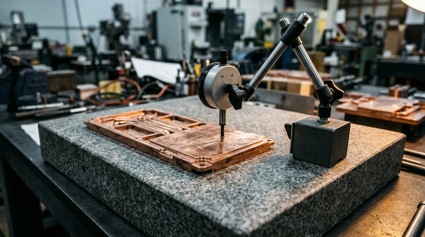
Flatness is measurable, and the method should be named in the drawing. A granite surface plate with a dial indicator resolves about 0.01 mm; a coordinate measuring machine gives a full map and is the better choice when you need to know the shape, not just the peak deviation. Measure over the die footprint, not only over the whole plate: a plate can be flat overall and dished exactly where the die sits.
One more thing to specify: flatness after reflow. A chamber is a sealed pressure vessel, and its internal pressure rises with temperature, so a plate that measures flat at 25 °C can bow during a 260 °C excursion and cool into a different shape. If the assembly goes through reflow, ask for flatness measured after the full thermal cycle, not only at incoming inspection. The same logic applies to pads: thickness and compression decide what the layer does under load, and a pad specified by nominal thickness alone is only half specified.
Pressure, Pump-Out and What Ages First
Mounting load sets the bond line, and more load is not automatically better. The thin shell deforms under point loads: a screw boss or a clip directly over the die can dent the wall, pinch the vapor cavity and create a low-conductivity patch that no interface material can fill. The usual fix is structural — a stiffening frame, screws placed away from the die, a controlled torque — and it should be settled before the interface material is chosen, because it sets the bond line the material will see.
Grease ages in two ways, and neither is visible on day one. Pump-out is driven by the mismatch in thermal expansion between the materials either side of the layer: as the stack heats and cools, the two faces move relative to each other, squeezing the grease outward, and the return stroke does not pull it back. Dry-out is the separation of filler from polymer at temperature, leaving a dried residue with poor conduction. Both end the same way — voids, higher interface resistance, a junction temperature that drifts upward over a qualification campaign.
Phase-change materials are the common middle path: solid at room temperature, fluid above a transition that for the TIC®800 family sits at 50–60 °C. The first power cycle melts and thins the layer, and because the material re-wets on each cycle it resists pump-out better than a grease that only flows once. The cost is a dependence on that first cycle — a phase-change interface that never gets hot enough never reaches its design bond line.
Pads and gap fillers take the opposite trade. They tolerate larger and less uniform gaps and need little pressure, which is why they are common on the large faces inside a server chassis; the price is a thicker layer and the resistance that comes with it. Liquid metal gives the lowest bulk resistance of any option here, at 35 W/m·K, and brings the strictest assembly rules: it must be contained, it cannot sit against aluminum mating faces, and being electrically conductive it cannot be allowed to bridge. Choosing between the families is its own decision — gap filler, gap pad or phase-change material lays out the boundary — but the chamber adds one constraint to all of them: the surface it meets is thin, and it moves.
Failure Modes and the Tests That Catch Them
Qualification plans often test the chamber and the interface separately and never test the joint. The failures below are joint failures, so the test has to see the joint.
| Failure | Where it starts | Test that catches it | What to ask for |
|---|---|---|---|
| Pump-out, dry-out | TIM1 or TIM2 | power cycling with in-situ junction temperature | resistance at cycle 0, 500 and 1,000, same power and load |
| Voiding, delamination | die attach, TIM2 | scanning acoustic tomography or cross-section | void fraction at the die corners, not the average |
| Capillary limit reached | wick at the far evaporator edge | power sweep in the worst mounting orientation | maximum power versus orientation curve |
| Non-condensable gas, leak | seal, fill tube | fine leak test plus performance drift | leak rate limit and the method used to measure it |
| Deformation, dent | thin wall under a screw or clip | flatness map before and after assembly | flatness over the die footprint |
| Starved interface | die corner with a bowed plate | cross-section bond line at center and corner | bond line distribution, not one average value |
The single most useful line in a supplier report is a resistance value with the pressure, the bond line and the method attached. A number without them cannot be compared to the competitor's number, and comparing the two is usually the reason the report was requested.
Matching the Interface Material to the Interface
No single family wins all four interfaces in the table above. ZIITEK's published ranges map roughly like this, and the watch-out column is the part that decides field behavior:
| Family | k (W/m·K) | Interface it fits | Watch |
|---|---|---|---|
| TIF® pads | 1.25–16, 0.25–12 mm | TIM2 across an uneven or stepped gap | thickness adds resistance; not a 50 µm play |
| TIG®780 grease | 1.0–5.2 | thin bond line where rework matters | pump-out under cycling; dispense control |
| TIC®800 phase change | 0.95–9.6, 0.127–0.508 mm, 50–60 °C transition | TIM2 where grease pumps out | needs a first cycle hot enough to melt and thin |
| TIR®700 carbon fiber | 9–25 | thin, low-pressure, electrically non-insulating | conductive and tack-free; containment matters |
| Liquid metal | 35 | extreme flux, fully contained | aluminum mating faces, electrical bridging |
| TIF® gels, one- and two-part | 1.5–9.0 | high-bond-line gap fill, near-zero stress | not a thin-bond-line interface |
These are datasheet ranges. A conductivity range without the pressure, bond line and test method behind it describes a material rather than an interface, so confirm those conditions against your joint before you design to it.
For a grease specifically, the TIG®780 grease range carries the viscosity and dispense options; the selection question is whether the joint will be reworked in the field or sealed for life, because that single answer eliminates half the table.
What to Send With the RFQ
A supplier cannot choose a material from a die size alone. The eight inputs that change the answer:
- Die footprint, power and the resulting heat flux at the contact face.
- Chamber flatness and the measurement method, over the die footprint and over the full plate.
- Target bond line, and the tolerance you will accept on it.
- Mounting load, the hardware that applies it, and where the load lands.
- Whether the assembly goes through reflow, and at what peak temperature.
- The cycling profile the part will see in qualification: range, dwell, number of cycles.
- Electrical isolation requirements, which decide whether liquid metal or a conductive pad is even admissible.
- The test method and acceptance limit you will use to accept the first article.
Send those and the material conversation starts at the second question instead of the first. ZIITEK supplies the interface materials in this stack — grease, phase-change film, pads, gels — not the chamber itself, so the useful conversation is about the joint rather than the plate. If the eight inputs above are already on your desk, send them to the thermal engineering team and they will come back with a material and a test plan.
Frequently Asked Questions
Does a vapor chamber replace thermal paste? No. It replaces the base of the heat sink, or in some builds the lid. The paste, film or pad between the die and the chamber — and between the chamber and the sink — is still there, and it is still the layer with the highest resistance per unit of thickness.
What is the difference between TIM1 and TIM2? TIM1 sits between the die and the first spreader, so it sees the smallest area and the highest heat flux. TIM2 sits between the spreader and the next level of hardware, so it sees a larger, less uniform gap and the mounting load. They usually need different materials.
Can a thermal pad be used against a vapor chamber? Yes, most often at TIM2, where a pad absorbs gap variation and needs little pressure. Two constraints apply: the pad's thickness adds resistance, and its compression load has to be compatible with a thin chamber wall that can dent under a point load.
Why does thermal grease lose performance after cycling? Pump-out and dry-out. The faces either side of the grease expand differently, so each cycle squeezes material outward without pulling it back; at temperature the polymer can also separate from the filler. Both leave voids, and the junction temperature rises as a result.
How flat does a vapor chamber surface have to be? Most chambers are held to better than 0.1 mm as built, and thin-bond-line designs need tighter. The number that matters is the deviation over the die footprint, not over the whole plate, and it should be measured after any reflow the assembly sees.