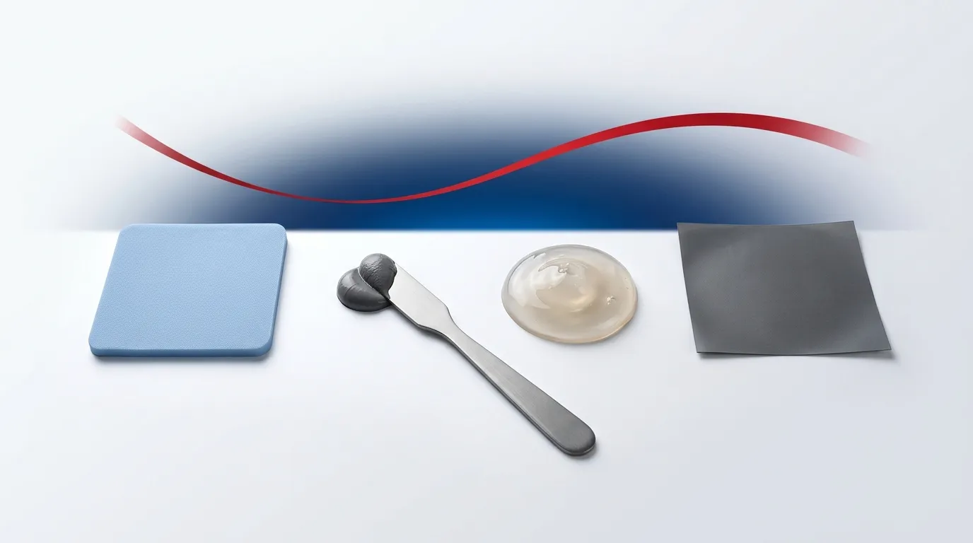
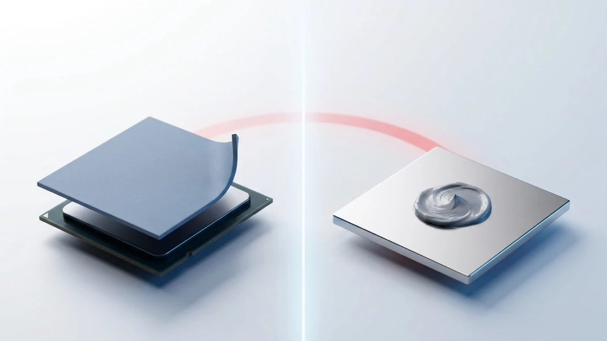
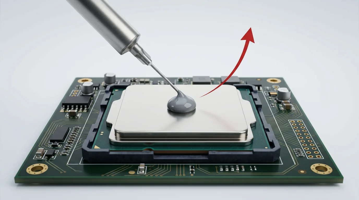
Gap Filler vs Gap Pad vs Phase Change Material
Gap fillers conform to large, uneven gaps; gap pads are the fastest drop-in; PCM gives the lowest resistance on flat, high-power lids. A design-in comparison.
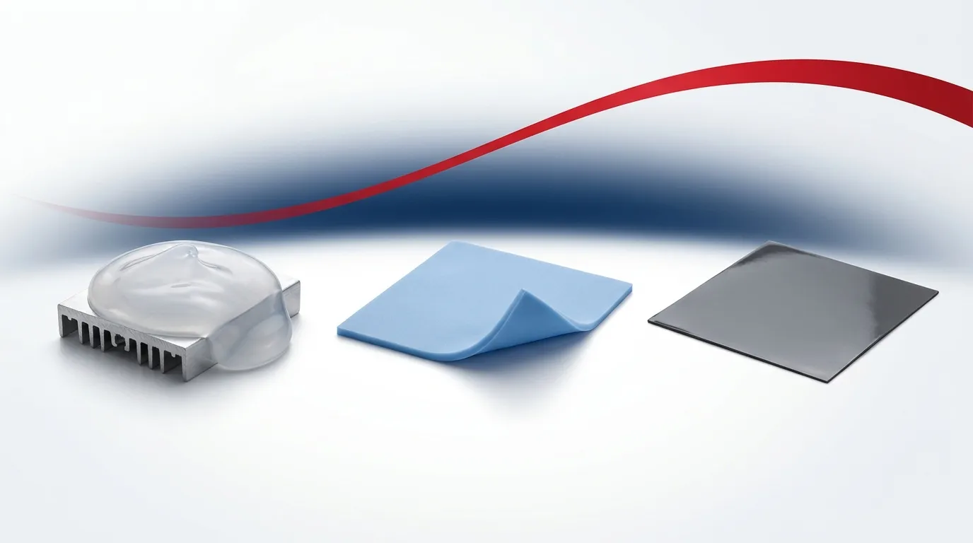
Three materials, one job: fill the microscopic air gap between a hot component and its heatsink so heat can actually cross the joint. A thermal gap filler, a thermal gap pad, and a phase change material (PCM) all do that — but they behave so differently in your line, your reliability lab, and your BOM that picking the wrong one shows up later as slow takt time, cracked BGAs, or field failures nobody caught in qualification.
The confusing part is that datasheets make them look interchangeable. They quote thermal conductivity in W/m·K, list a thickness, and stop. In reality the choice turns on how each material deforms, how it goes onto the part, and how it ages — not on which one has the biggest number. This guide compares all three across the criteria that actually decide a design-in, gives you a decision framework, and maps each material to real end-markets. It’s the head-to-head companion to our complete thermal interface material selection guide.
The 30-second answer
- Choose a gap filler when the gap is large, uneven, or varies part-to-part, when the component is fragile (thin PCB, BGA), or when you want to automate a dispensing line. It conforms to almost anything at near-zero mounting stress.
- Choose a gap pad when you want the simplest, cleanest, most reworkable option for a defined, repeatable gap — pick it up, place it, clamp it, done. No dispensing equipment, no cure.
- Choose a phase change material when the interface is flat, thin, and high-power (a CPU/GPU lid or IGBT baseplate), and you want the lowest steady-state thermal resistance without the pump-out risk of grease.
Here is the same decision as a side-by-side matrix.
Comparison table: gap filler vs gap pad vs phase change
| Criterion | Thermal gap filler (dispensable) | Thermal gap pad (pre-cured sheet) | Phase change material (PCM) |
|---|---|---|---|
| Form | Liquid/gel paste, 1- or 2-part, cures or stays soft | Solid compressible die-cut sheet | Solid film at room temp; melts and wets at operating temp |
| Bulk k — datasheet range\* | ~1.5–9.0 W/m·K (ZIITEK TIF® gel) | ~1.25–16 W/m·K (ZIITEK TIF® pad; 9–35 for carbon-fiber types) | ~0.95–9.6 W/m·K (ZIITEK TIC®800) |
| Gap / bond-line range | ~0.2 mm to several mm; conforms to variation | ~0.3–5 mm, fixed nominal thickness | Very thin, ~20–100 µm on flat lids |
| Mounting stress on parts | Very low | Moderate–high (needs clamp force) | Very low after melt |
| Assembly method | Robotic/manual dispense | Pick-and-place, peel-and-stick | Pre-applied/screen-printed or die-cut pad, then burn-in |
| Reworkable? | Cured filler no; soft gel partial | Yes — peel and replace | Partial (softens when hot) |
| Main reliability watch-item | Pump-out (1-part), cure control | Compression set, rated k needs rated pressure | First-power-up wetting, re-melt cycling |
| Best-fit gap | Large, uneven, tolerance-heavy | Defined, repeatable, needs service access | Flat, thin, high heat flux |
* These are ZIITEK’s own catalog ranges, shown to indicate roughly what each format can span — not an industry survey, and deliberately not a cross-vendor comparison. Read them as “what shape of number to expect,” nothing more. As the next section argues, a bulk k figure is not comparable to another bulk k figure unless both are stated with the test pressure and bond-line thickness they were measured at — which is exactly why this table does not rank the three by conductivity.
Now the reasoning behind each row — because the table tells you what, and a design review needs why.
The three materials, in one line each
A thermal gap filler is a dispensable, thermally conductive gel or two-part liquid (also called a form-in-place TIM). You dispense it as a paste; it flows to fit the surface, then either cures in place or stays as a soft, compliant putty. It is the shape-shifter of the group. ZIITEK’s TIF® gel line sits here at roughly 1.5–9.0 W/m·K.
A thermal gap pad is a pre-cured, compressible silicone (or silicone-free) sheet, die-cut to shape. You pick it up and place it. It’s the plug-and-play option, and the one most people mean by “thermal pad.” If you want the fundamentals of pad construction and how thickness is specified, see what is a thermal pad.
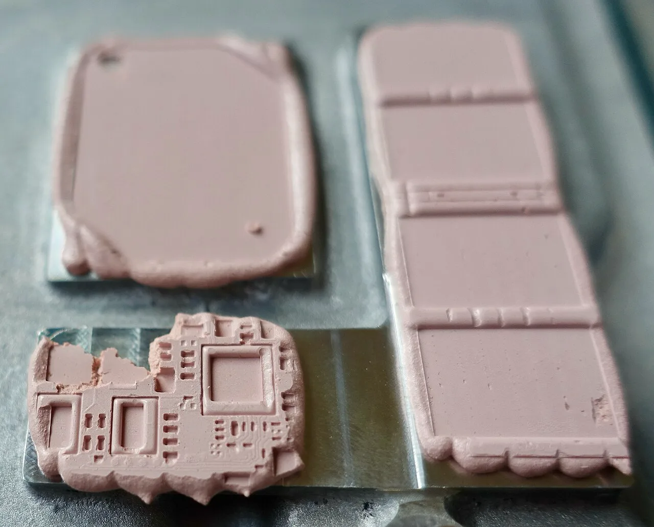
Photo by Steve Jurvetson via Wikimedia Commons.jpg>), CC BY 2.0
A phase change material is solid and easy to handle at room temperature, then melts around 45–65 °C — during the product’s first power-up — and wets the interface like a grease that can’t run away. That transition is the whole point, and it’s the part every competing article glosses over; we unpack it in what is phase change material (PCM) TIM. ZIITEK’s TIC®800 PCM transitions at 50–60 °C.
Thermal performance: stop comparing raw W/m·K
The single most common mistake in TIM selection is ranking materials by datasheet conductivity. Bulk conductivity (k) is a material property; what your junction actually feels is thermal resistance across the whole joint:
R″ ≈ (bond-line thickness ÷ k) + contact resistance
A pad rated 6 W/m·K sitting at 1.5 mm can present more resistance than a 3 W/m·K filler that squeezes down to 0.2 mm and wets both faces with zero air voids. Thickness and surface wetting frequently beat raw k. This is also why PCM — despite a middling k — often wins on a flat CPU lid: it forms an extremely thin, void-free bond line that neither a pad nor a thick filler can match. If the impedance-versus-conductivity distinction is fuzzy, our explainer on thermal resistance vs thermal impedance walks through the math, and understanding thermal conductivity (W/mK) covers where the k number comes from.
Two disciplines make the comparison honest:
- Demand ASTM D5470 data. The ASTM D5470 through-plane method is how credible suppliers measure TIM impedance. A k value is only comparable if it’s stated with the test pressure and bond-line thickness it was measured at.
- For pads, remember rated k requires rated pressure. A gap pad only reaches its datasheet conductivity when it’s compressed to the specified deflection. Under-clamp it and the real resistance climbs. Fillers and post-melt PCM don’t carry this asterisk because they wet the surface at near-zero pressure.
Mechanical stress and component safety
This is where gap pads lose points and fillers shine. A pad only performs when it’s compressed — typically 10–50% of its thickness — and that deflection generates reaction force on whatever is clamping it. On a stiff assembly that’s fine. On a thin PCB, a large module, or a fragile BGA, that force warps boards and stresses solder joints. Harder, higher-k pads are the worst offenders.
Dispensable gap fillers apply almost no mounting stress: the paste flows into place and needs only enough pressure to reach the target bond line. PCM is similar once it melts. So when the mechanical budget is tight — sensor modules, large flat lids over delicate silicon, thin-FR4 assemblies — the low-stress materials (filler, PCM) are the safer structural choice, even if a pad looks simpler. Compression behavior is a topic in its own right; see the thermal pad thickness & compression guide for how deflection targets are set.
Gap size and tolerance stack-up
Before anything else, check which regime your gap is in — because the three materials barely overlap on the one axis you can measure with a feeler gauge.
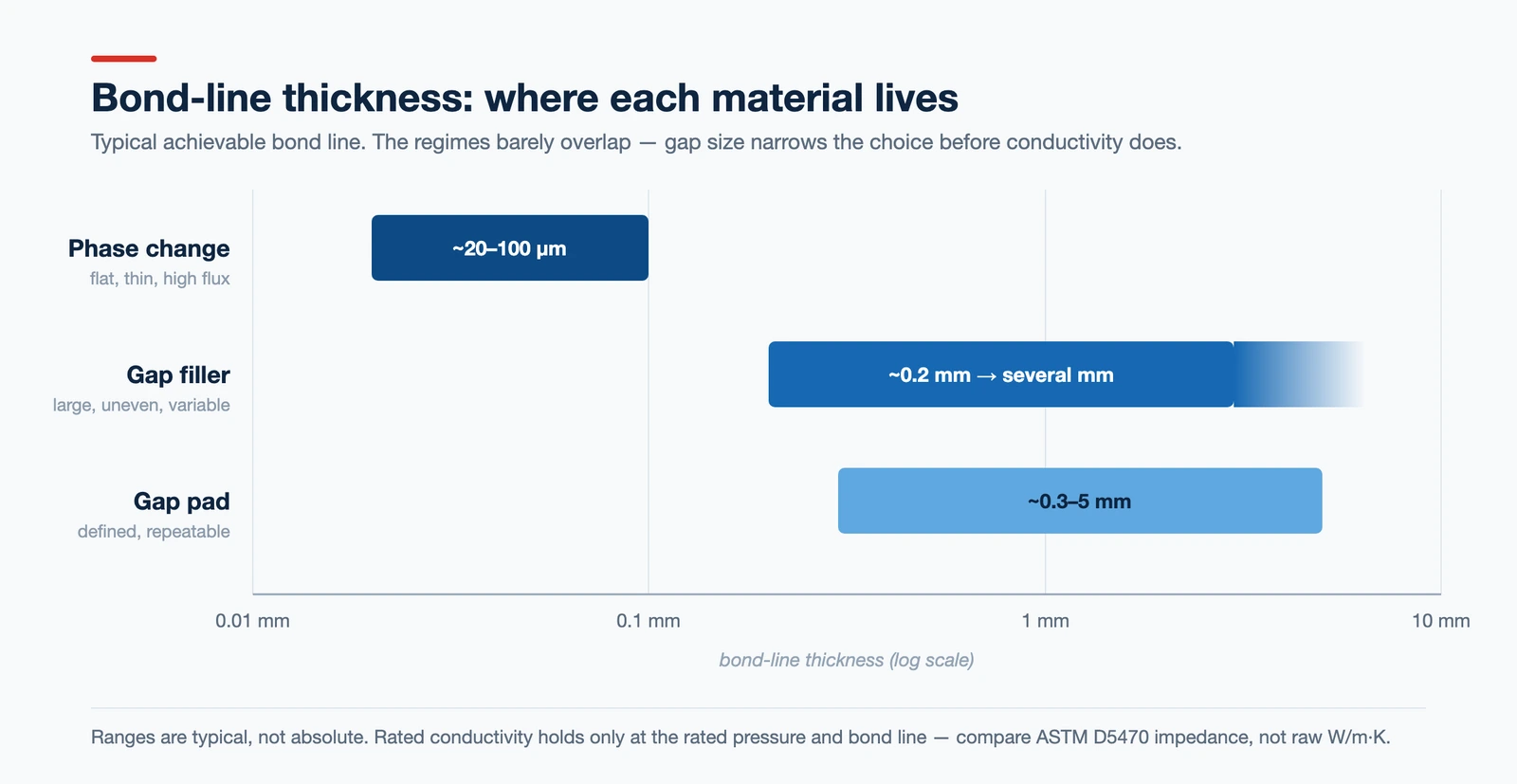
Real assemblies don’t hold a perfect, uniform gap — tolerance stack-up across the housing, PCB, and heatsink means the “1 mm gap” is really 0.6–1.4 mm across a batch. Each material handles that differently:
- Gap filler absorbs variation for free. Dispense a controlled volume and it fills whatever gap the parts present, part to part. This is why fillers dominate where gaps are large or inconsistent.
- Gap pad comes in fixed nominal thicknesses. To cover a variable gap you either over-compress (more stress) or leave air (worse resistance). Stacking two pads to reach a big gap is a common anti-pattern — it adds two more contact interfaces and usually raises resistance.
- PCM is for the opposite regime: thin, flat, well-controlled interfaces measured in tens of microns, not millimeters.
Assembly, automation, and throughput
Form factor decides how the material rides down your line:
- Gap pads are the throughput champion for manual or pick-and-place assembly: no equipment, no cure, no cleanup. Tape-and-reel and peel-and-place kits drop straight into existing flows.
- Gap fillers shine at high-volume automation: a robotic dispenser lays down a precise bead in seconds, no die-cut tooling, easy to change the pattern when the design revs. The trade is capital (a dispenser) plus nozzle maintenance and void inspection.
- PCM is often supplied with sheet format, which is extremely clean for the assembler — but it needs a burn-in / first-power-up step to melt and wet before it hits rated performance. If your takt time can’t absorb that, factor it in.
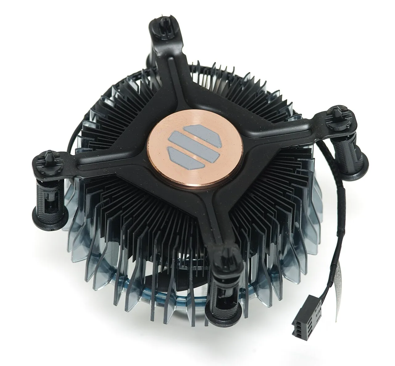
Photo by Ashley Pomeroy via Wikimedia Commons, CC BY 4.0
Reworkability and field serviceability
If a unit will be opened for service, rework, or upgrade, this row can override everything else. Gap pads win: peel the old one off, drop a new one in. Cured gap fillers lose: they’re effectively permanent, and removing one is messy. PCM is in between — it softens when warm and can be replaced, but it isn’t as clean as a pad. High-mix, repairable, or field-serviceable products lean toward pads for exactly this reason.
Reliability: pump-out, compression set, and outgassing
Steady-state numbers hide the failure modes that show up 1,000 thermal cycles later. The three materials fail in different ways:
- Pump-out is the classic risk for one-part fillers (and greases): repeated expansion/contraction slowly walks the material out of the joint, leaving voids. Two-part cured fillers and PCM resist this far better — PCM re-solidifies each cool-down and stays put.
- Compression set is the pad-specific ager: a pad that’s held under load for years can take a permanent set and lose contact pressure, raising resistance.
- Outgassing matters for optics, sensors, and sealed enclosures. Silicone materials can release low-molecular-weight siloxanes; if that’s a concern, specify a silicone-free option and screen it against ASTM E595 (TML ≤ 1.0%, CVCM ≤ 0.1%) — NASA’s public outgassing database is a useful reference for how materials are rated.
Qualification should cover thermal cycling (e.g., −40 → 125 °C), damp heat (85 °C / 85% RH), dielectric strength if the TIM is also an insulator, and flammability — UL 94 V-0 is standard for most electronics. For a plain-language primer on the material family, Wikipedia’s thermal interface material entry is a reasonable starting point. One warning if you go reading further: Wikipedia’s phase-change material entry describes the same physics put to a completely different job — storing thermal energy in buildings and packaging, not thinning a bond line. It’s useful background on the phase transition itself, but it is not about PCM as a thermal interface material, and conflating the two is the single most common source of confusion on this topic.
Cost and total cost of ownership
Per-gram or per-sheet pricing is misleading. Count the whole picture:
- Gap pads: low material and labor cost at moderate volume; inventory cost if you carry many thicknesses; waste from die-cut skeletons.
- Gap fillers: material can be cheaper per joint at scale and there’s near-zero geometric waste, but you pay for the dispenser (capital), maintenance, and cure/cycle time.
- PCM: material cost is moderate; the hidden cost is the burn-in step and tighter surface-flatness requirements.
At low-to-medium volume, pads usually win on TCO. At high volume with automation already in place, dispensed fillers often pull ahead. PCM earns its cost only where its thermal edge on a hot, flat interface is worth it.
Match the material to your application
| End-market | Typical interface | Usual best fit |
|---|---|---|
| EV / ESS battery packs | Large, uneven cell-to-coldplate gaps; stress-sensitive modules | Gap filler — conforms, low stress, dispensable at volume |
| Servers / AI data center | Flat high-power CPU/GPU lids; some large board-level gaps | PCM on the lids; gap filler/pad for board-level gaps |
| Power electronics (IGBT, modules) | Flat baseplate to heatsink, high heat flux | PCM or high-k filler |
| Telecom / 5G | RF module lids, mixed gaps, sealed enclosures | Gap pad (serviceable) or low-outgassing filler |
| ADAS / ECU / automotive | Thin PCBs, vibration, wide temp range | Gap filler for low stress and vibration damping |
These are starting points, not verdicts — your gap, your stress budget, and your rework requirement still govern, in that order. But notice how often the answer is not “the highest W/m·K product.” Our broader walk-through, how to choose a thermal interface material, extends the same logic to greases and tapes.
When NOT to use each
Vendor product pages rarely tell you this, so here it is plainly:
- Don’t use a gap pad to bridge a large or highly variable gap by stacking or heavy over-compression — you’ll add interfaces or over-stress parts.
- Don’t use a cured gap filler where the unit must be opened and reworked — you’re building in a permanent joint.
- Don’t use PCM where the interface isn’t flat and thin, or where production can’t accommodate a burn-in step.
- Don’t use any silicone TIM near optics/sensors without checking outgassing — specify silicone-free.
How to spec it right
Before you commit, put every candidate on equal footing:
- Get ASTM D5470 impedance curves, each point tagged with test pressure and bond-line thickness — not a lone k number.
- For pads, get the conductivity at your actual deflection, and the clamp force that deflection implies.
- Ask for reliability data at your conditions: thermal cycling, 85/85, and pump-out/compression-set results.
- If outgassing matters, require ASTM E595 (or better) data and consider silicone-free chemistry.
- Confirm UL 94 V-0 and any dielectric requirements.
A supplier that can hand you all of that quickly is telling you something about their engineering discipline.
Where ZIITEK fits
As a thermal-materials manufacturer, ZIITEK makes all three families, which means the recommendation isn’t captive to one format:
- TIF® gel / gap filler (dispensable, ~1.5–9.0 W/m·K) for large, uneven, low-stress gaps and automated lines.
- TIF® gap pads (~1.25–16 W/m·K) for defined, reworkable gaps.
- TIC®800 PCM (~0.95–9.6 W/m·K, transition 50–60 °C) for flat, high-power lids that need the lowest resistance.
Note that the PCM has the lowest headline conductivity of the three — and is still the right answer on a flat, high-power lid, because it wins on bond-line thickness and wetting, not on k. That’s this entire article in one line, and it’s why we publish the number rather than quietly omitting it.
The TIF® gel and TIF® pad lines carry UL 94 V-0 recognition under ZIITEK’s UL Yellow Card (E331100); for a PCM grade, ask for the flammability rating on that specific datasheet rather than assuming the company-level listing covers it. Across the range, materials are RoHS/REACH compliant and produced under IATF 16949 / ISO 9001 processes, and are benchmarked as drop-in alternatives to common incumbents. If you’re speccing for a specific gap, thermal budget, and assembly method, request samples, datasheets with ASTM D5470 curves, or engineering support for your design.
FAQ
What’s the difference between a thermal gap filler and a gap pad? A gap filler is dispensed as a liquid/gel that conforms to the gap and then cures or stays soft; a gap pad is a pre-cured solid sheet you place and compress. Fillers handle large, uneven, or variable gaps at low mounting stress; pads are simpler to assemble and easy to rework but need clamp force and come in fixed thicknesses.
Is a phase change material better than a gap pad or gap filler? For a flat, thin, high-power interface (like a CPU/GPU lid), PCM usually gives lower thermal resistance and better pump-out resistance than grease, and a thinner bond line than a pad. For large or uneven gaps, a filler or pad is the right tool — PCM only shines on thin, flat, well-controlled joints.
What is a phase change thermal pad, and does it need burn-in? It’s a PCM supplied in pad form. It’s solid at room temperature and melts on first power-up (around 45–65 °C) to wet the interface — so yes, it reaches rated performance only after that first thermal excursion (the “burn-in”).
What are thermal gap pads made of? Typically a silicone (or silicone-free) polymer matrix loaded with ceramic fillers such as alumina, boron nitride, or aluminum nitride, sometimes with a fiberglass or film carrier. Filler type and loading set the conductivity, hardness, and electrical behavior.
Which is better for high-volume automated assembly, a gap filler or a gap pad? Dispensable gap fillers suit high-volume automation — a robot lays a precise bead with no die-cut tooling and easy pattern changes. Pads are excellent for manual or pick-and-place lines and need no dispensing equipment. The tie-breaker is whether you already have (or want) a dispenser, and whether rework is required (favoring pads).
Can I use thermal putty instead of a pad? Thermal putty is essentially a soft, non-curing gap filler — it conforms like a filler with low stress and no dispenser needed for small runs, but it’s messier to rework and doesn’t offer a pad’s clean handling. It’s a reasonable middle ground for uneven gaps in low-to-medium volume.
How do gap fillers and PCM compare to thermal paste? Thermal paste (grease) gives a very thin bond line but is prone to pump-out and dry-out over time. PCM offers grease-like thinness without the pump-out; fillers and pads trade some thinness for the ability to span real gaps. See thermal pad vs thermal paste for that head-to-head.