Thermal Pad Thickness & Compression Guide
Thermal pads only reach their rated W/mK under compression, usually 20–30%. Learn to measure the gap, pick nominal thickness, and set the right mounting force.
Choosing thermal pad thickness looks like a one-number decision, but it is really two decisions working together: the nominal thickness you order and the compression it sees once the assembly is torqued down. The short answer: target 20–30% compression, and always order a pad thicker than your largest gap — roughly 1.25× it. Get the pairing wrong and a pad rated at 6 W/mK can behave like one at 2 — or, at the other extreme, bow the PCB and crack a solder joint. This thermal pad thickness and compression guide walks through how to measure the gap, pick a nominal thickness, hit the right compression ratio, and set a mounting force your board can actually survive.
It is written for hardware, mechanical, and thermal design engineers specifying a gap pad into a product, though the same physics applies whether you are cooling a data-center GPU or replacing VRAM pads on a graphics card. For the broader landscape of gels, greases, and phase-change films, start with our thermal interface materials selection guide; this article zooms into the one variable pads live and die by.
Why compression is the whole point
A thermal pad’s job is to displace the air trapped between two imperfect surfaces. Air conducts heat at roughly 0.026 W/mK, while filled silicone gap pads run about 1.25–18 W/mK — roughly 50× to 700× better, two orders of magnitude — so any air left in the interface dominates the thermal path. A pad only pushes that air out and wets both surfaces when it is squeezed. The datasheet’s headline thermal conductivity is measured on a fully compressed sample; install the same pad loose and you never see that number.
This is the single most common field mistake, and it shows up in enthusiast testing too: a 1 mm pad compressed to 0.6 mm (40% compression) hits its rated performance, while the same pad barely touching the heatsink does not. If you only remember one thing from this guide, remember that thickness and compression are specified as a pair — a nominal thickness is meaningless until you know how much of it will be squeezed away. (New to pads entirely? Our primer on what a thermal pad is covers the fundamentals before you spec one.)
Step 1 — Measure the gap accurately
Everything downstream depends on knowing the real distance between the heat source and the cold surface (the heatsink, chassis wall, or cold plate). Do not eyeball it.
- Feeler gauges — slide leaves into the gap until you find a snug fit. Fast on the bench, ±0.05 mm at best.
- Digital calipers / depth micrometer — measure the standoff height and subtract component height. Good for single, well-defined gaps.
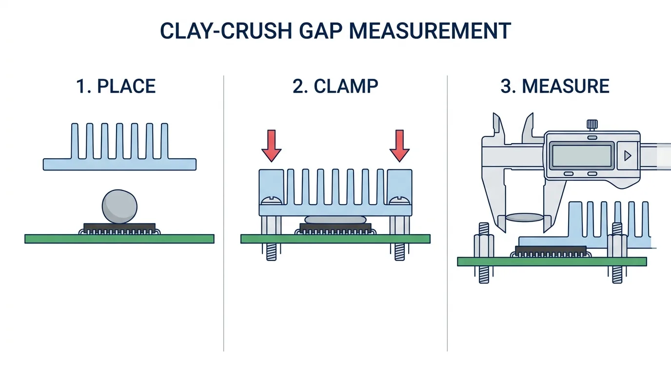
- Clay or soft-putty crush test — place a ball of modeling clay, close the assembly to its final torque, reopen, and measure the flattened clay thickness with calipers. This captures the real clamped gap including board flex — the most honest single-point method on a prototype.
- Coordinate measuring machine (CMM) or height gauge — for production tolerancing and co-planarity across multiple components under one heatsink.
Account for tolerance stack-up. The nominal CAD gap is not the gap every unit will have. Add up the worst-case tolerances of the component height, PCB warp, standoff, and heatsink flatness. If your nominal gap is 1.0 mm but stack-up gives you 0.7–1.4 mm across production, you must choose a pad that performs across that whole window, not just at nominal. Soft pads forgive stack-up; that forgiveness is exactly what you are buying.
Check co-planarity when one heatsink spans several chips of different heights. Each site may need a different pad thickness, or you accept uneven compression and design the softest pad that still contacts the shortest component.
Don’t forget surface finish. The “gap” is not just the bulk distance — it includes the microscopic roughness of both faces. A machined heatsink base typically runs about 0.8–3.2 μm Ra; extruded or as-cast surfaces are rougher. That roughness is what the pad must flow into to displace the last of the air, and it is why a soft pad at modest compression often beats a firm one at high compression on the same gap.
Step 2 — Choose the nominal thickness
Pick the thinnest pad that reliably fills your worst-case gap. Thinner is thermally better (more on why in the impedance section), so you want just enough thickness to guarantee contact plus compression — not more.
There is no lookup table that can do this for you, because the answer depends on your gap window, not on a nominal number. But there is a two-line rule you can apply to any stack-up. Compression at a given gap is simply:
Compression % = (nominal thickness − gap) ÷ nominal thickness × 100
Which gives the sizing rule:
- Size for the LARGEST gap. The pad must still be meaningfully squeezed at your worst-case maximum gap — that is the unit where contact is lost first. Targeting ~20% compression there: nominal ≈ maximum gap ÷ 0.8 (i.e. 1.25 × your max gap). Round up to the nearest catalog thickness.
- Then check the SMALLEST gap. Recompute compression at your minimum gap. If it exceeds ~40%, you are pushing into high-reaction-force territory — see the deflection section below.
The non-negotiable output of step 1: nominal thickness must always exceed your maximum gap. If nominal ≤ max gap, the pad at that gap is at zero or negative compression — it is not touching the heatsink at all, and that unit has no thermal path. Any chart that lists a nominal thickness equal to or below the top of its own gap range is describing a part that does not work.
Worked examples of the rule, using common catalog thicknesses:
| Gap window (min – max) | Nominal thickness | Compression at MAX gap | Compression at MIN gap |
|---|---|---|---|
| 0.18 – 0.24 mm | 0.3 mm | 20% | 40% |
| 0.30 – 0.40 mm | 0.5 mm | 20% | 40% |
| 0.60 – 0.80 mm | 1.0 mm | 20% | 40% |
| 0.90 – 1.20 mm | 1.5 mm | 20% | 40% |
| 1.20 – 1.60 mm | 2.0 mm | 20% | 40% |
| 1.80 – 2.40 mm | 3.0 mm | 20% | 40% |
| 3.00 – 4.00 mm | 5.0 mm | 20% | 40% |
Check any row yourself: a 2.0 mm pad in a 1.60 mm gap is squeezed to 1.60 mm → (2.0 − 1.6) ÷ 2.0 = 20%. The same pad in that design’s tightest 1.20 mm unit → (2.0 − 1.2) ÷ 2.0 = 40%. Both bounds land inside the working window, which is the whole point.
Read those two columns as the extremes across your production spread, not as a target. The unit at your nominal gap sits between them — around 30% for these rows, right in the sweet spot covered in Step 3. What matters is that the worst unit in either direction is still safe: none starved of contact, none crushed.
How wide a stack-up can one thickness absorb? Falling out of the derivation above: holding every unit between 20% and 40% needs your minimum gap to be at least 75% of your maximum gap. Open the accepted window to 10–50% and one pad covers a min/max ratio down to about 0.56. Wider than that and no single nominal thickness exists that keeps every unit in the window — you are choosing between over-compressed units and units with no contact.
That is a real constraint, not a rounding note. Return to the Step 1 example: a stack-up of 0.7 – 1.4 mm has a ratio of 0.50. Filling 1.4 mm at ≥10% compression needs nominal ≥ 1.56 mm; keeping the 0.7 mm units under 50% compression needs nominal ≤ 1.4 mm. Those cannot both be true. That stack-up cannot be solved with a die-cut pad — tighten the tolerances, split into per-site thicknesses, or move to a dispensable gap filler that conforms to whatever gap each unit presents. See gap filler vs gap pad vs phase change for that trade-off.
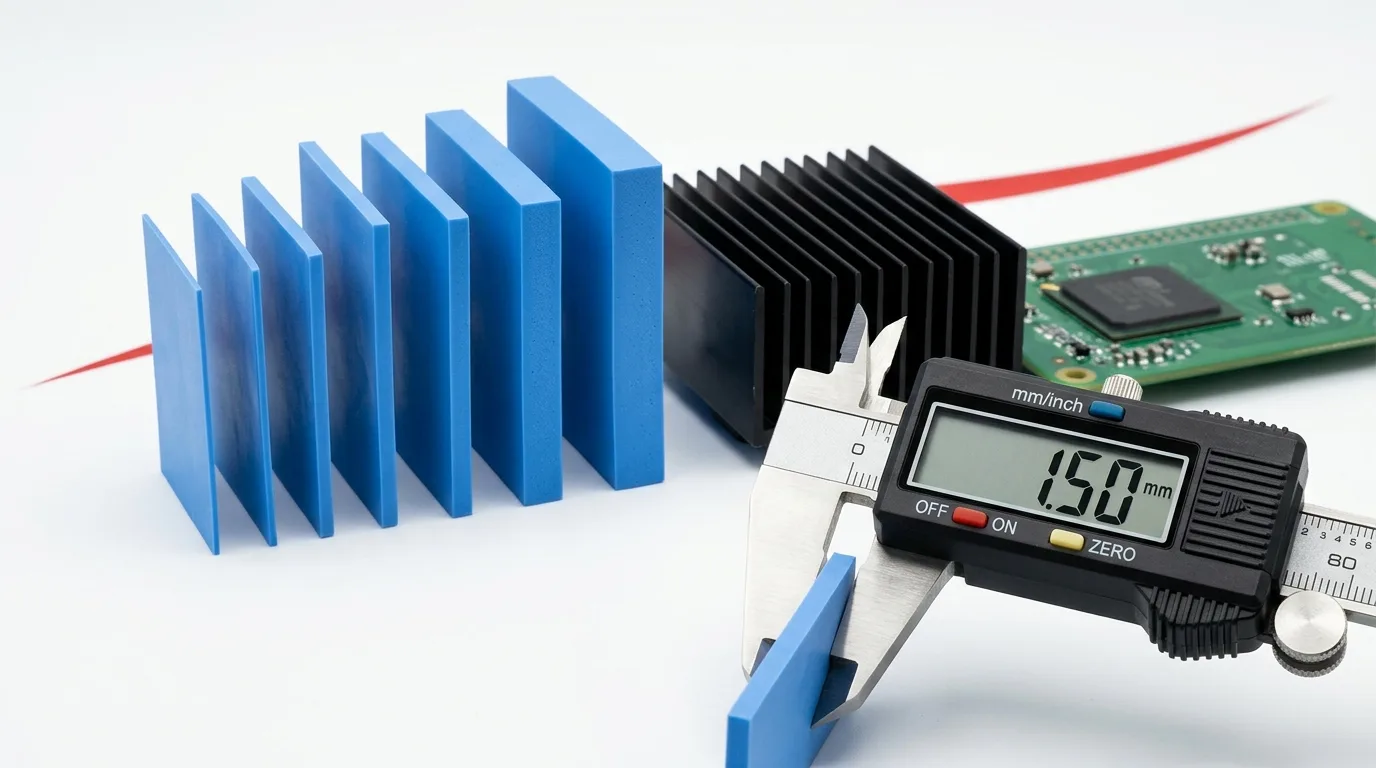
Note the gaps between the rows above (0.40–0.60 mm, 0.80–0.90 mm, and so on). Catalog thicknesses do not tile the gap axis continuously — when your window falls between two rows, go up one thickness and re-run the arithmetic at both bounds rather than assuming it works. Confirm the result against the pad’s actual datasheet, since deflection behavior varies by formulation. ZIITEK’s TIF® silicone gap pads run from 0.25 mm up to 12 mm, so one series covers everything from an SSD controller to a battery-module gap.
Step 3 — Hit the right compression ratio
Compression ratio is how much the pad’s thickness is reduced at final assembly, as a percentage of its nominal thickness. A 2.0 mm pad squeezed to 1.5 mm is at 25% compression.
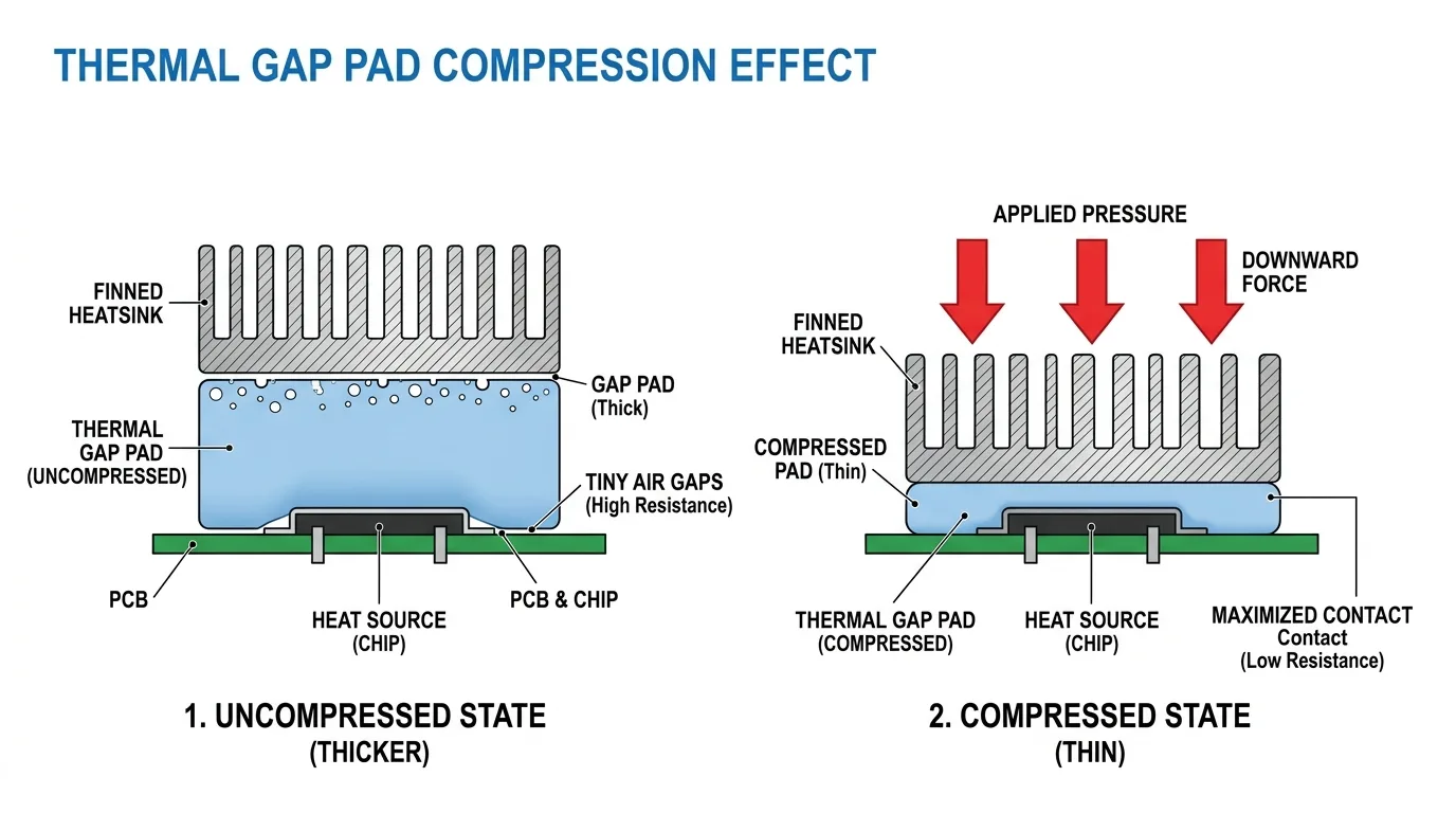
The workable window across most silicone gap pads is roughly 10–50%, and 20–30% is the sweet spot for the majority of designs. Below ~10% you often leave micro-air-gaps and never reach rated conductivity; push past ~50% and you generate large reaction forces without much extra thermal gain, while risking the mechanical problems covered below. Softer, higher-conductivity pads tolerate the upper end; firm, reinforced pads should stay lower.
Two rules keep you out of trouble:
- More compression always lowers thermal resistance — until it doesn’t. The impedance-vs-compression curve is steep early (squeezing out air) and flattens fast. The jump from 5% to 25% buys a lot; the jump from 40% to 55% buys almost nothing but a lot of force.
- Design to the compression, not the gap. Specify the pad so that at your maximum gap you still get enough compression to contact, and at your minimum gap you do not exceed the pad’s safe deflection.
Deflection force and mounting pressure
Here is where most guides go quiet, and where designs actually fail. Compressing a pad takes force, and that force pushes back on your board and hardware.
Deflection force (or mounting pressure) is the pressure needed to hold the pad at a given compression, expressed in kPa or psi. It rises with compression percentage and — steeply — with pad stiffness.
We are deliberately not quoting a single “typical” kPa figure here, because there isn’t one. Compression-versus-stress is not a property of “gap pads” as a class; it is a property of one formulation at one thickness at one temperature, and it varies by an order of magnitude across the soft-to-reinforced range. Three things are reliably true and worth designing around:
- The curve is non-linear and it stiffens. Pressure climbs gently through the early compression range and then rises sharply as the elastomer runs out of room. The last 10% of compression can cost more force than the first 30%.
- Hardness is the dominant variable. A low Shore OO pad reaches useful compression at a small fraction of the pressure a firm, fiberglass-reinforced pad needs at the same percentage.
- Only the datasheet curve is authoritative. Suppliers characterize this with a compression-deflection test — the rubber-industry method is ASTM D575, which loads a specimen and records force against deflection. Ask for the stress-strain or deflection-vs-pressure curve for your grade at your thickness, and read your operating point off it. If a supplier cannot produce that curve, you cannot predict what the pad will do to your board.
Why over-compression is dangerous:
- PCB bowing. Excess reaction force flexes the board. Over thermal cycles that flex fatigues solder joints under BGAs — a failure that shows up months later as intermittent faults, not on day one.
- Component and die stress. Bare-die parts, ceramic capacitors, and LED emitters can crack under point loads from an over-thick, over-stiff pad.
- Fastener and standoff creep. High sustained reaction force relaxes screws and plastic standoffs, and the clamp load — and your compression — drifts down over time.
Practical guidance: size the pad so the required clamp load fits what your fasteners and board can carry, then verify the resultant thickness rather than assuming the screw torque delivers it. When the allowable clamp load is low (thin PCBs, delicate optics), prioritize a soft, low-deflection pad over a higher-W/mK but stiffer one — the softer pad’s better real-world contact usually wins. This force-versus-conductivity balance is a core part of how to choose a thermal interface material.
Shore OO hardness — the spec everyone forgets
Pad softness is quantified by Shore OO hardness (durometer, per ASTM D2240) — the scale used for very soft, gel-like materials such as gel seat cushions and soft silicones, well below the Shore A range used for firmer rubbers. On the Shore durometer scale, a lower OO number means a softer, more conformable pad.
Hardness is the hidden lever behind deflection force:
- Low Shore OO (soft, ~5–25): conforms to rough or non-flat surfaces at low pressure, forgives tolerance stack-up, and protects fragile components. Trade-off: less mechanically robust, more prone to tearing on install, and usually tackier — natural surface tack helps a pad stay put during assembly but makes rework messier and can lift a pad off its liner in automated placement.
- High Shore OO (firm, ~50–70): holds shape, handles and die-cuts cleanly, survives vibration — but demands more clamp force and is less forgiving of uneven gaps.
Hardness is largely set by the filler system. Gap pads are silicone (or silicone-free) binders loaded with ceramic filler — typically alumina for general-purpose grades, or boron nitride where a lower dielectric constant and lighter weight matter. Higher filler loading buys W/mK and costs conformability: the highest-conductivity grade in a family is almost never its softest.
ZIITEK’s TIF® pads span roughly 5 to 70 Shore OO, letting you trade conformability against robustness without changing supplier. Whenever a datasheet omits hardness, treat that as a gap in the spec and ask for it — you cannot predict mounting force without it.
Is a thicker thermal pad better? Thickness vs thermal impedance
No. This is the most persistent myth in pad selection. The number that governs real cooling is thermal impedance — the temperature drop across the interface per unit heat and area (°C·cm²/W), not the bulk conductivity alone.
Total interface impedance is, simplified, the material’s bulk resistance plus the two contact resistances at each surface:
Impedance ≈ (bond-line thickness ÷ thermal conductivity) + contact resistance
Contact resistance is roughly fixed once the pad wets the surfaces, so impedance grows almost linearly with bond-line thickness. This is exactly how TIMs are characterized under ASTM D5470: measure one material at several thicknesses and plot impedance against thickness. The plot is a straight line whose reciprocal slope gives the thermal conductivity, and whose zero-thickness intercept gives the total contact resistance (myheatsinks explains the method here, and the ASTM D5470 standard defines the test).
The takeaway for design: use the thinnest pad that still fills your worst-case gap with adequate compression. Extra thickness “for safety” directly adds thermal resistance.
What to do when you need both a large gap and low impedance. Reaching for a high-W/mK pad is the instinct, but check its thickness range before you specify it. High-conductivity carbon-fiber pads — ZIITEK’s TIR®700 (9–35 W/mK) among them — are thin-gap parts: the TIR®700 line runs roughly 0.3–5 mm, and the highest-conductivity grades are the thinnest. They are the right answer for a thin interface that needs maximum conductivity at low pressure, and the wrong answer for a 3 mm chassis gap. Two further cautions on carbon-fiber pads: TIR®700 is electrically conductive (non-insulating) — never place it where the pad is also the isolation barrier, which rules it out of most of the datasheet checklist below; and its high-conductivity grades are firmer (65–85 Shore OO), so they conform less than a soft silicone pad. If the gap is genuinely large and the interface must insulate, the honest answer is usually a soft silicone gap pad at a modest W/mK, or a dispensable gap filler — not a thin, conductive, high-W/mK part forced into a role it was not built for. For the full treatment of these two metrics, see thermal resistance vs thermal impedance and understanding thermal conductivity (W/mK).
Don’t stack pads to fill a big gap. Two 1 mm pads are not one good 2 mm pad — you add an extra air-prone interface in the middle and roughly double the risk. Specify a single correct thickness instead.
When not to use a pad at all
A guide about pads should say where pads lose. Three cases:
- Very thin, flat, high-power interfaces (a bare die or lidded CPU to a cold plate). At a few tenths of a millimetre, a pad’s bulk resistance is hard to beat with a grease or a phase-change film that achieves a much thinner bond line. Pads win on serviceability and cleanliness, not on raw impedance here.
- Large gaps with wide variation — the case Step 2 proves a single pad cannot solve. A dispensable gap filler conforms to whatever each unit presents, at near-zero stress.
- Very low allowable clamp load with an uneven gap. If the board cannot take the reaction force a pad needs, a gel or filler that cures in place is the safer path.
ZIITEK supplies pads, gels, greases, and phase-change film, so this is a materials question rather than a loyalty one: pick the class that fits the interface, then optimize within it.
Long-term behavior: compression set, relaxation, and cycling
A pad that is perfect on day one can drift. Three mechanisms matter over a product’s life:
- Compression set — after long compression the pad does not fully rebound; if the clamp load ever eases, contact can be lost. Quality silicone pads keep set low, but it is real.
- Stress relaxation — the reaction force decays over time at fixed compression. Combined with fastener creep, this lowers effective mounting pressure and can raise impedance years in.
- Thermal cycling — repeated expansion and contraction works the interface and can drive slow degradation. (This is analogous to the “pump-out” that afflicts greases, one reason pads are chosen for high-cycle designs.)
Design margin for these: don’t sit at the extreme low end of the contact window at beginning-of-life, and favor materials with published low compression set for sealed, long-service, or automotive-qualified products. ZIITEK’s pads run to a working range of typically −40 °C to 200 °C depending on grade, under an IATF 16949 and UL 94 V-0 (UL Yellow Card E331100) quality system, for exactly these reliability-driven applications.
Thickness and compression by application
The gaps below are the range across designs in each category — not one design’s stack-up. Read the thickness column the same way: it is the Step 2 rule (nominal ≈ 1.25 × that site’s own max gap, rounded up) applied across the low and high end of the gap range. A site at the 0.5 mm end of the SSD row wants a 0.7 mm pad; a site at the 0.2 mm end wants 0.3 mm. Never pair the bottom of the thickness column with the top of the gap column — that is the zero-compression trap.
| Application | Typical gap range | Nominal thickness (per site, ≈1.25 × that site’s max gap) | Notes |
|---|---|---|---|
| SSD controller / laptop VRM | 0.2 – 0.5 mm | 0.3 – 0.7 mm | Thin, flat, low tolerance — keep impedance minimal |
| GPU VRAM / VRM pads | 0.5 – 2.0 mm | 0.7 – 2.5 mm | Mixed heights under one plate — size each site separately |
| High-power CPU/GPU to cold plate | 0.2 – 1.0 mm | 0.3 – 1.5 mm | Prioritize high W/mK + low impedance |
| Power electronics / IGBT modules | 1.0 – 3.0 mm | 1.5 – 4.0 mm | Larger, uneven gaps; watch clamp load on ceramics |
| EV battery / ESS modules | 1.0 – 5.0 mm | 1.5 – 6.0 mm | Big variable gaps — often past the single-pad ratio limit; gap filler frequently wins |
| LED / lighting | 0.3 – 1.5 mm | 0.5 – 2.0 mm | Protect emitters — soft, low-pressure pad |
Use the table as a starting envelope, then run Steps 1–3 — including the min/max ratio check — for your specific stack-up.
How to read a pad datasheet
Before you commit, confirm the datasheet reports all of the following — if any is missing, ask the supplier:
- Thermal conductivity (W/mK) and, ideally, thermal impedance at a stated pressure and thickness (the number that predicts real performance).
- Available nominal thicknesses and thickness tolerance.
- Shore OO hardness and a deflection-force / stress-strain curve.
- Compression set and operating temperature range.
- Dielectric strength if the pad also insulates, plus compliance (UL 94, RoHS/REACH).
A datasheet that lists only “W/mK” and thickness is telling you less than half the story.
FAQ
How much should a thermal pad be compressed? Most silicone gap pads work best at 20–30% compression, within a usable range of about 10–50%. Below ~10% you risk residual air gaps; above ~50% you add mounting force with little thermal benefit.
Is a thicker thermal pad better? No. Thermal impedance rises roughly linearly with thickness, so the thinnest pad that still fills your worst-case gap under adequate compression performs best. Use higher conductivity, not more thickness, to solve a large gap.
Can I stack two thermal pads to fill a bigger gap? Avoid it. Stacking adds an extra internal interface prone to trapped air and doubles the failure surfaces. Specify one pad of the correct thickness instead.
How do I measure the gap for a thermal pad? Use feeler gauges or a depth micrometer for a quick read, or a clay-crush test (close to final torque, then measure the flattened clay) to capture the real clamped gap including board flex. Always add tolerance stack-up.
What is Shore OO hardness and why does it matter? Shore OO is the durometer scale for very soft materials. A lower number means a softer, more conformable pad that needs less mounting force — critical for thin PCBs and fragile components.
Specify with confidence — and get engineering support
Thermal pad selection is a paired decision: measure the real gap, choose the thinnest nominal thickness that fills it, target 20–30% compression, and verify the mounting force your board can carry. Nail those four and you get rated performance without cracking a joint.
ZIITEK designs and manufactures thermal interface materials for OEMs across EV/ESS, servers, telecom, and power electronics, including the TIF® gap pad line (1.25–18 W/mK, 0.25–12 mm, 5–70 Shore OO), carbon-fiber TIR®700 pads, and silicone-free Z-Paster®100. If you are dialing in thickness and compression for a specific stack-up, the two numbers to bring to any supplier are your gap window (min and max, from a real clamped measurement) and your allowable clamp load. With those, matching a pad is a short conversation — and our engineering team can pull the datasheet, the deflection curve for the specific grade, and samples in your thickness. To see how gap pads sit against gels, greases, and phase-change films across the whole decision, read the thermal interface materials selection guide.
Sources
- ASTM D5470-17(2024), Standard Test Method for Thermal Transmission Properties of Thermally Conductive Electrical Insulation Materials — the standard defining TIM thermal-impedance testing.
- ASTM D575-91(2018), Standard Test Methods for Rubber Properties in Compression — the compression-deflection method behind a pad’s deflection-force curve.
- ASTM D2240 / Shore durometer scale — the Shore OO hardness scale and its typical materials.
- MyHeatsinks, Thermal Interface Material Test — Based on ASTM D5470 — the impedance-vs-thickness method: contact impedance from the zero-thickness intercept, conductivity from the reciprocal of the slope.