Thermal Pad Thickness for Heat Sink Gaps
The gap under a consumer-device heat sink is a tolerance band, not one number. Size thermal pad thickness from both bounds, then check hardness and clamp force.
What a Thermal Pad for a Heat Sink Has to Do in a Consumer Device
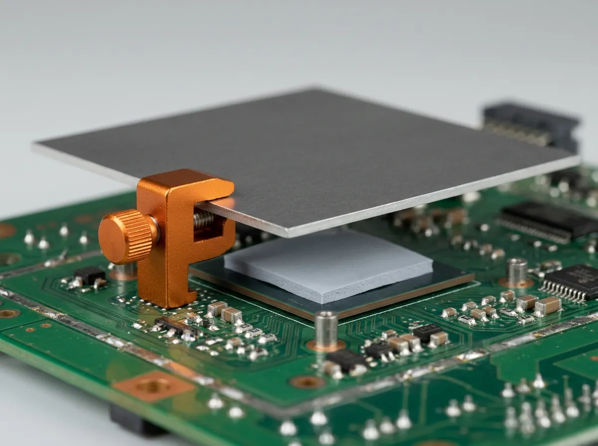
A thermal pad for a heat sink — the flat, die-cut sheet often sold as a thermal gap pad — is a ceramic-filled silicone part that bridges the mechanical gap between a hot component and a metal surface. Its job is narrower than "conducting heat": it has to displace the air in that gap. Air conducts at roughly 0.026 W/mK, while a filled silicone pad runs from 1.25 to 16 W/mK across ZIITEK's TIF range, so whatever air survives the assembly dominates the thermal path no matter how good the pad is.
In a consumer device the metal on the other side is thin. It is a drawn shield can over a mainboard, a die-cast chassis wall, a stamped bracket, or a plate that also serves as the product's back cover. Three things follow from that, and they are what separates this problem from data-center cold-plate work:
- The gap is short. Consumer stacks mostly land between about 0.2 mm and 1.5 mm, a range where catalog thickness increments are coarse relative to the gap.
- The clamp force is small. Clips, adhesive tape and two or four small screws cannot deliver the pressure a bolted cold plate can.
- The gap varies across the part. Stamped and die-cast surfaces are not flat, and the board they sit on is not flat either.
The general theory of thermal pad compression — the measurement instruments, the standard thickness ladder and the mounting-force calculation — lives in the compression and thickness guide. This page is the operating sequence for one specific situation: a thin heat sink over a real component in a device you are about to tool, where the question is not what compression means but which thickness to order, and how to prove it fits before you commit. If you are still deciding whether a pad is the right material at all, the primer on what a thermal pad is covers the fundamentals.
The Gap Is a Band, Not a Number
Every decision about thermal pad thickness for heat sink gaps starts with a measurement, and the most common mistake is treating the CAD number as the gap. It is the gap for exactly one unit — the nominal one, which is the unit you will never build.
Four contributors move the real gap away from nominal in a consumer assembly:
| Contributor | What moves it | Working range |
|---|---|---|
| Component height | Package and lid tolerance, die-attach and mold height | ±0.02 to ±0.05 mm |
| Board flatness | Reflow warp, copper balance, panel handling | ±0.03 to ±0.10 mm across a heat-sink footprint |
| Heat-sink base | Stamp or casting flatness, coating thickness | ±0.02 to ±0.05 mm |
| Standoff / tape | Screw boss height, adhesive tape thickness, clip geometry | ±0.02 to ±0.05 mm |
Those ranges are working estimates taken from consumer-device stack-ups, not values from a standard; replace them with your own DFM data before you size anything. What matters for the method is that each contributor is independent and additive, so the band is the sum.
Add them worst-case and you have the band the heat sink thermal pad has to survive. Take a mid-range phone mainboard: 0.45 mm nominal gap, ±0.03 mm package, ±0.06 mm warp, ±0.03 mm base flatness, ±0.03 mm standoff. That is ±0.15 mm, or a 0.30–0.60 mm band. The nominal number is 0.45 mm; the band runs 33% below it and 33% above it, and no single pad thickness covers that range — as the next section shows.
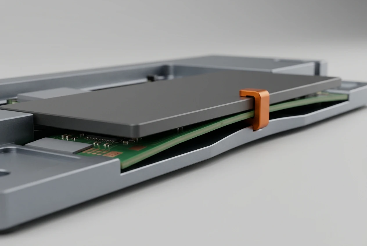
If you are working on a module rather than a whole device, the same logic applies at a smaller scale — the M.2 SSD pad selection guide walks through a stack where the controller, the NAND and the shield all present different heights under one cover.
From Band to Thickness: Two Bounds and a Window
Thermal pad compression is the variable that ties the two numbers together. As a fraction it is (nominal thickness − actual gap) ÷ nominal thickness, and a pad is only correct when both ends of the band land inside the window you accept.
For a thin heat sink on a low-force assembly, use a 15% floor and a 40% ceiling. (A general guide often quotes a 20% floor, because a bolted cold plate can be trusted with more force; on a thin heat sink under a light clip, 15% is the honest floor and the 40% ceiling does not move.) The floor is contact: below roughly 15% you are touching the high points and hoping. The ceiling is mechanics: past about 40% the pad generates reaction force faster than it improves the interface, which on a thin chassis or an unsupported board is how PCBs bow and snap fits pop. The 20–30% middle of that window is where most designs should land at nominal.
Short answer. Size from both ends of the band: the pad must be at least max gap ÷ 0.85 for contact and no more than min gap ÷ 0.60 for load. A single thickness exists only while max ÷ min stays at or under about 1.42.
Two inequalities follow:
- At the maximum gap, 15% compression requires
t ≥ max gap ÷ 0.85. - At the minimum gap, 40% compression allows
t ≤ min gap ÷ 0.60.
Applied to the 0.30–0.60 mm band: t ≥ 0.706 mm and t ≤ 0.50 mm. There is no thickness that satisfies both, because the band is wider than the window can absorb. The general form of that condition, and a catalog ladder to pick from once a window exists, are worked through in the compression guide; what follows is how it plays out on a real stack.
Partial tightening rarely gets you there. Cut the warp to ±0.03 and hold the base to ±0.02 and the stack goes from ±0.15 to ±0.11 — a 0.34–0.56 mm band with a min ÷ max ratio of 0.61, still short of the 0.706 that a 15–40% window needs. (Both inequalities can hold only when min ÷ max ≥ 0.60 ÷ 0.85 = 0.706.) You have to attack the band until it clears, not until it looks better.
Now run the same arithmetic on a taller gap — three of the four rows already at the bottom of their range, and a shield can sitting 0.60 mm above a camera module:
| Constraint | Calculation | Result |
|---|---|---|
| Gap band | 0.60 mm nominal, ±0.10 (0.03 + 0.03 + 0.02 + 0.02) | 0.50 – 0.70 mm |
| Contact at max gap (≥15%) | 0.70 ÷ 0.85 | t ≥ 0.824 mm |
| Safe load at min gap (≤40%) | 0.50 ÷ 0.60 | t ≤ 0.833 mm |
| Feasible window | 0.824 – 0.833 mm | 0.83 mm, on paper only |
| Check at 0.70 mm | (0.83 − 0.70) ÷ 0.83 | 15.7% |
| Check at 0.50 mm | (0.83 − 0.50) ÷ 0.83 | 39.8% |
| At nominal 0.60 mm | (0.83 − 0.60) ÷ 0.83 | 27.7% |
A 10 µm window is not a specification. No die-cut part is held to that, and the incoming thickness tolerance you are told to check in the last section is several times larger than the window itself: at ±0.05 mm the same bought-in part delivers 10.3% at the 0.70 mm unit, which is below the contact floor, and 43.2% at the 0.50 mm unit, which is over-compressed. Even ±0.005 mm still lands at 40.1% at the tight end. No stocked increment rescues it either — 0.75 mm gives 6.7% at the wide end and 0.85 mm gives 41.2% at the tight end.
So this band does not clear in production. On paper it does, and only just: a min ÷ max ratio of 0.714 against the 0.706 the window demands. That is the most useful result in this article, and it points the same way as the last section. The 0.45 mm stack runs a 50% ratio because its tolerance is a third of its gap; this 0.60 mm one reaches 71% because a smaller ±0.10 mm tolerance is only a sixth of a taller gap — the tolerance shrank and the gap grew, and both moved the ratio the same way. Neither stack is a thickness-shopping problem. Tighten the window to the 20–30% middle instead and even this band has no solution: t would have to be at least 0.875 mm at the 0.70 mm unit and no more than 0.714 mm at the 0.50 mm one.
When No Single Thickness Covers the Band
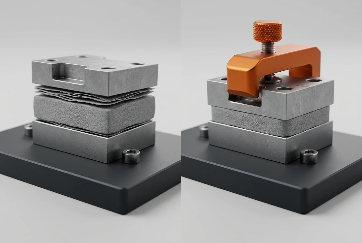
The 0.30–0.60 mm case is not a corner case. It is what a stamped heat sink over a large, thin board looks like before anyone has thought about thermal, and the first response is usually to look for a cleverer thickness. There isn't one.
The order in which you attack it matters, because the cheap moves are mechanical and the expensive one is a material change:
- Kill the largest contributor first. Rank the four rows of the band table by size and attack the top one. On most consumer boards that is warp, and the fix is geometry — stiffener ribs under the footprint, a boss, more mounting points, or a shorter span between screws. Halving warp does more than halving any other row.
- Then take the base out of the problem. A machined or coined base face and a controlled coating thickness beat a stamped surface every time, and they cost a machining step rather than a redesign.
- Only then split the thickness per site. If the band still will not clear, give each site its own thickness — covered in the section after next, and the answer that usually survives a real device with several components under one plate.
- Last, change the material form. A dispensable gap filler conforms to whatever gap each unit presents, at the cost of a cure step and a dam. The comparison of the three families is in gap filler versus gap pad versus phase change.
What you should not do is average the band and specify the midpoint. That guarantees the widest units have no contact and the narrowest ones are over-compressed, and both failures are invisible in a first-article inspection that happens to draw a nominal unit.
Thickness You Can Actually Close: Hardness and Clamp Force
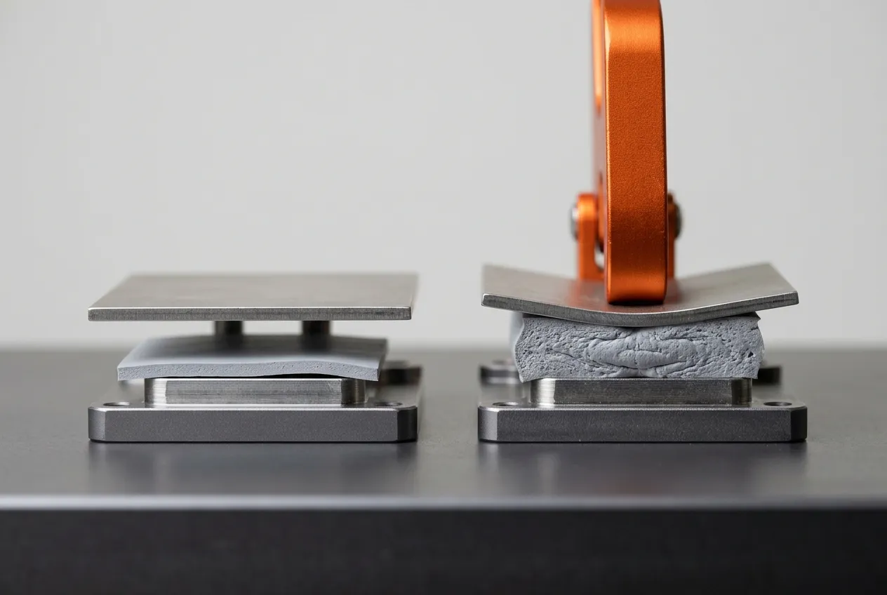
A thickness only counts once the assembly can compress it. In a consumer device the force comes from a snap fit, a piece of tape, or two M2 screws into plastic — a fraction of what a bolted cold plate applies, and frequently the binding constraint rather than the gap.
Thermal pad hardness is what converts that available force into deflection, and it decides whether the thickness you picked for your band reaches 15% compression or sits on the high points. ZIITEK's TIF pads span 5 to 70 Shore OO over a 0.25–12 mm thickness range, and the spread exists because the same thickness behaves completely differently at the two ends: a 70 Shore OO pad may barely deflect under a light clip, while a 5–25 Shore OO pad at the same thickness conforms to the same gap and makes contact.
The uncomfortable part is that hardness is rarely specified the way it needs to be: a bare Shore OO number is not a design input. Ask for the deflection at your assembly pressure, and if the supplier cannot give it, test a sample in your own fixture — the mounting-force arithmetic for that is in the compression guide.
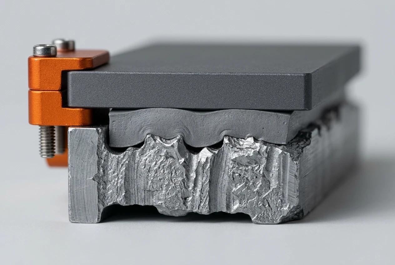
Soft is not automatically safer in the other direction, either. A very soft, very thick pad under a tight clip can bottom out and transmit the full load, which puts you back in the reaction-force problem the softness was supposed to solve. Thickness and hardness have to be specified as a pair against a stated assembly force, and the pair has to be checked at both ends of the band.
One Heat Sink, Several Components: Per-Site Thickness
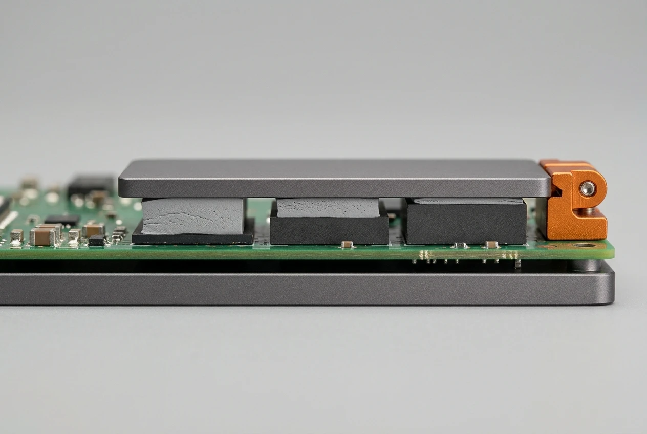
Consumer devices rarely have one gap. A single shield can or plate typically covers an SoC, a power management IC, a memory package and sometimes a connector — the same arrangement of a CPU or GPU and its supporting components that a laptop or a console presents — each at a different height, and the plate is flat while the components are not co-planar.
Two failure modes come out of that geometry, and they are not symmetric:
- The tallest component sets contact. It takes the load first, so the plate tilts or the board flexes and the shorter sites end up with no compression at all.
- The shortest component sets over-compression. If you size one pad for the short site, the tall site is crushed and its reaction force is what the clip has to hold.
The practical answers are per-site die-cut thicknesses, local bosses or pedestals that bring sites onto one plane, or a deliberately soft pad that can absorb the height difference without loading the tallest part. This is a converting problem as much as a material one: ZIITEK runs 30-plus automatic cutting and die-cutting machines across four plants, so cutting and die-cutting capacity is not the constraint — the drawing is, and the wider selection logic for these device stacks is collected in the consumer electronics thermal pad hub.
Thin Beats Conductive: The Resistance You Add by Filling
Thickness is not free, and the cost is easy to compute for the bulk material: R = t ÷ k. Compare a 0.50 mm pad at 3 W/mK with a 1.50 mm pad at 6 W/mK:
| Pad | Thickness | Conductivity | Bulk resistance |
|---|---|---|---|
| A | 0.50 mm | 3 W/mK | 1.67 × 10⁻⁴ m²·K/W |
| B | 1.50 mm | 6 W/mK | 2.50 × 10⁻⁴ m²·K/W |
The thinner, half-as-conductive pad wins by about a third. In a thin device that ordering is the design instruction: the optimization direction is a thinner bond line, not a higher k. Doubling conductivity does not pay for tripling thickness.
Contact resistance works against that ordering — at 0.5 mm the interfaces can be most of the total, and a softer pad that wets both surfaces can beat a thin firm one — and the datasheet k only exists under compression, so quote the pressure and bond-line thickness that came with any impedance figure (ASTM D5470 is the method behind most of them).
Where the device is thin and the flux is high, the material choice moves rather than the thickness. ZIITEK's TIF100N uses boron nitride for a lower dielectric constant where capacitance between traces matters. The TIR700 carbon-fiber family runs 9–25 W/mK, with the 25 W/mK formats starting at 0.30 mm, thin enough for a narrow gap. It is electrically conductive and has no adhesive of its own, so it belongs on a grounded surface or under a shield, never bridging two different potentials and the 9 W/mK grade spanning 0.75–5.00 mm; the 2026 manual lists the two upper formats of that family as 85/60 Shore OO against a 0.30–0.50 / 1.00–5.00 mm thickness map without saying whether the values pair positionally, so check the exact format's datasheet before you design to either reading.
Two more options belong on the list. ZIITEK's Z-Paster100 is a non-silicone pad rated 1.5–10 W/mK over 0.25–5.0 mm for silicone-sensitive assemblies — set-top boxes, power supplies, LED and optical modules — where siloxane outgassing is the problem, and the TIF100L low-volatile grade (1.5–6.0 W/mK, 0.25–5.0 mm) covers the same concern inside the silicone family, which is the one specified for cameras, security and laser equipment.
Proving the Choice Before Tooling
Before committing tooling, three checks catch most thickness errors, and all three are cheap on a handful of units:
- Witness marks. Assemble, disassemble, and look at the pad. A full, even imprint on both faces means contact; a patchy imprint or a shiny uncompressed ring means the pad is too hard or too thick at that site.
- Cross-section. Pot or clamp a unit, cut through the stack, and measure the actual bond-line thickness under a microscope. This is the only way to see whether the pad compressed to the number you designed and whether the void you were worried about is still there.
- Incoming thickness tolerance. The thickness on your drawing is a nominal, not a delivered value; the supplied tolerance eats directly into your window. Put the thickness and its tolerance on the drawing and measure a sample on receipt.
The stack also changes over time. A pad takes compression set after thermal cycling and vibration, so the interface you qualified at nominal compression is not the one you ship at month eighteen — ASTM D395 is the compression-set method, and how long thermal pads last covers what that means over a product life.
Hardness is measured the same way: Shore OO values come from the ASTM D2240 durometer method, and a supplier quoting a hardness without a scale is quoting nothing you can design to.
The specification that comes out of all of this fits on one line per site:
- Gap band, min and max, with the four tolerance contributors listed so the supplier can see what they are absorbing.
- Nominal thickness plus tolerance, and the compression window you expect at both ends of the band.
- Hardness in Shore OO, with the assembly force or clip type stated.
- Thermal conductivity and the impedance figure, with the test pressure and bond-line thickness if either is quoted.
- Flame rating — UL 94 V-0 is the common requirement in consumer electronics, and it should be tied to the actual listing rather than to a generic claim.
- Form: die-cut outline, adhesive on one face or none, and whether the part needs a tab for rework.
A pad that meets the thickness window but not the hardness, or the hardness but not the tolerance, will fail in production rather than in the lab. Getting both on the drawing the first time is what avoids a second tooling round; if the stack-up is still open, send it to us and we will size it against the thermal pad range before you cut anything.