Conformal Coating vs Potting for Drone ESCs
Conformal coating vs potting for a drone ESC: compare the heat path to the housing wall, added mass, CTE stress and who pays for rework before you choose.
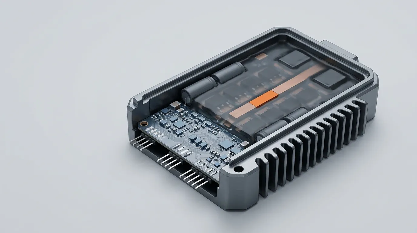
Conformal Coating vs Potting: Three Protection Options
A drone ESC has three protection options, not two, which is why conformal coating vs potting arguments miss the middle option. Coat the board when the housing already carries the environmental duty and the unit must stay serviceable and light. Pot a defined pocket around the power stage when heat has to reach an aluminum wall and nobody will open the unit in the field. Pot the whole board only when vibration or immersion dominates and the module gets discarded rather than repaired.
| Decision input | Coating | Local pot | Full pour |
|---|---|---|---|
| Thickness added | 25–250 µm | 2–6 mm | 5–15 mm |
| Heat path to wall | None; air gap remains | Direct, if the pocket reaches it | Direct, if the compound wets it |
| Dielectric margin | Surface only | Good | Best |
| Vibration, shock | Minimal | Local support | Whole-assembly support |
| Moisture, immersion | Film, not a seal | Seals the pocket | Seals the assembly |
| Inspection | Visual, UV tracer | Local, rest visible | X-ray or cross-section |
| Rework | Re-coat locally | Cut out and re-pour | Destructive |
| Choose it when | Housing seals; mass and repair matter | Hot cluster reaches the wall; unit never opens | Nothing serviceable; immersion dominates |
Most flight ESCs land on the middle column, with a thin thermal insulator under the MOSFETs. That answer is missing from most conformal coating vs potting comparisons, written by process sellers that rank protection levels: coating moderate, potting high. Protection level is not the design variable; three others are, all countable — junction-to-wall resistance, added grams, and who absorbs the repair.
Chemistry comes after architecture — which silicone, epoxy or urethane fills the volume is covered in the potting compound guide.
What Each One Physically Is
Conformal coating is a film: tens to a couple of hundred micrometers of acrylic, silicone, urethane, epoxy or parylene, sprayed, dipped or brushed on, following the board's topography. It is measured in microns because that is what it is — a moisture barrier that carries no load and spans no gap. Parylene is deposited from vapor, so it reaches under components instead of bridging over them.
Potting fills a volume. The assembly goes into a housing or mold, a two-part compound is poured around it and cures, and the housing becomes part of the product. Encapsulation is the same act with the mold removed afterwards. Its defining property is not more protection but that the air around components is replaced by a dielectric solid that is also a thermal and mechanical path.
The standards keep the two apart. IPC-CC-830B qualifies insulating compound for printed wiring assemblies, and its scope is a thin film on a test board — not a five-millimeter casting. A potting datasheet's hardness and conductivity describe a bulk material, not your joint. The family is indexed from the potting and encapsulation hub.
The ESC Thermal Path: Conformal Coating vs Potting
The generic comparisons skip this; for an ESC it decides the answer. Four MOSFETs at 3 W each — 12 W total — share a 600 mm² footprint, and conduction obeys R = t / (k·A).
| Layer between board and housing | Thickness | k (W/m·K) | R over 600 mm² |
|---|---|---|---|
| Air gap, board top to housing wall | 1.0 mm | 0.026 | 64 K/W |
| Silicone compound, TIS680-12AB | 3 mm | 1.2 | 4.2 K/W |
| Same compound, deeper pour | 6 mm | 1.2 | 8.3 K/W |
| Thermally conductive insulator under the device | 0.2 mm | 1.6 | 0.21 K/W |
| Conformal coating film | 0.1 mm | ~0.2 | 0.83 K/W |
The arithmetic is mine, not measured data, and 12 W through 64 K/W is a 768 K rise — a warning, not a design. The film's own 0.83 K/W is trivial beside it, which is why "coatings trap heat" is the wrong criticism and "coatings leave the gap alone" is the right one: a coating does not make an ESC hotter, it fails to make it cooler.
Potting closes it by construction, and then depth becomes the number you argue about: double the pour and you double the resistance, which is why a 2.8 or 3.5 W/m·K grade in the same series buys back roughly what doubling the depth costs. The silicone potting range runs 1.0 to 3.5 W/m·K over −45 to 200 °C; the 1.2 W/m·K grade is 65 Shore OO at 2.4 g/cm³, mixes 100:100 by weight, and carries a ≥6000 V/mm dielectric strength.
Two conditions decide whether it delivers. Wetting: a release agent on the machined face, or an anodized surface it will not key to, adds 0.08–0.83 K/W in series with the 4.2 K/W pour — a 2% to 20% penalty. An air pocket at the cavity floor reinstates the 64 K/W gap you meant to remove. Voids: a gas pocket in a high-field pour is where partial discharge starts, so degas and fill from one corner. Conductivity is a bulk figure from a specimen test (ASTM D5470), not a joint property.
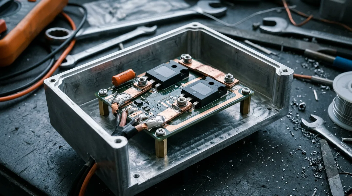
Weight and Rework Decide Earlier Than the Protection Spec
Both architectures protect. They differ in what they cost to carry and to fix, and both numbers are available before any material is chosen. At the potting compound's 2.4 g/cm³, on a 100 cm² board footprint:
| Approach | Material per 100 cm² | Added mass |
|---|---|---|
| Coating, 100 µm on both faces | ~2 cm³ at ~1 g/cm³ | ~2 g |
| Local pot, 12 cm² pocket × 6 mm deep | 7.2 cm³ | ~17 g |
| Full pot, 8 mm fill over the whole board | 80 cm³ | ~192 g |
That is arithmetic on assumed geometry, which is the point: without multiplying out the fill volume you cannot tell grams from hundreds of grams. On a 250 g class airframe, 17 g is about 7% of all-up weight and 192 g is about 77%; on a 3 kg airframe the same pour is about 6.4%.
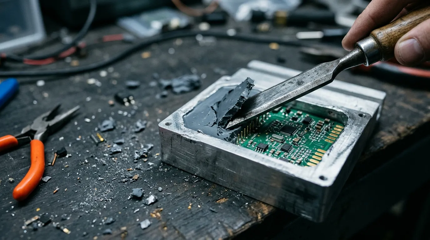
Rework separates them more sharply. A coated board is repaired by stripping the film locally — solvent or gentle abrasion, rework the joint, re-coat — provided the masking can be repeated. A locally potted board is repairable only if the pocket was designed for it: a wall around the compound, a release film or shallow step, clearance to cut it out without pulling a trace. Designed in, that is a five-minute repair; designed out, it is a destructive teardown.
A fully potted board is replace-not-repair: the compound is bonded to the housing and the assembly, and removing it without damaging the board is not a field operation. That suits a line-replaceable module with a spares multiplier; it does not suit a survey fleet where one failed gate driver would otherwise be a bench fix. Inspection follows the same split — UV tracer for a coating, X-ray or a sacrificial cross-section for a pour, which also costs mixing, degassing and cure time.
Stress: What a 65 Shore OO Silicone Buys, and What It Costs
Hardness is where the mechanical argument lives, and it is usually quoted without its scale. Shore OO, Shore A and Shore D are different instruments under ASTM D2240 and are not convertible; 65 Shore OO is a soft, compliant solid, while 65 on Shore D is a rigid one. Read as one scale, a soft gel gets specified where a structural fill was needed.
A soft compound transmits less load into solder joints and into the parts that crack first — large multilayer ceramics, heavy busbars, tall electrolytics — and lets board, copper and aluminum, three different CTE values, expand at their own rates without concentrating the mismatch at one interface. The costs: low tear strength, adhesion that usually needs a primer, no structural contribution.
Rigid systems, the filled epoxies at Shore D 70 and above, invert the trade: they bond without a primer, resist solvents and hold dimensions, which is why power modules default to them. The mechanism that bites is not "epoxy cracks" — a high-modulus material with a large expansion step transfers the mismatch into the stiffest interface, and a fast ramp beside a big ceramic or busbar edge is where a hairline starts.
Glass transition and exotherm work the same way. Below Tg a resin expands slowly; above it, several times faster with far less modulus, so a compound whose Tg sits under the hot-soak temperature is a different material in service. A system that gels in ninety minutes in a mixing cup can gel far sooner in a 500 g casting inside an insulated housing.

For a flight ESC the usual answer is a soft filled silicone, with a rigid epoxy potting compound reserved for modules that need that modulus — ZIITEK's TIE280 family covers 1.2 to 2.5 W/m·K over −45 to 130 °C with UL 94 V-0, against 1.0 to 3.5 W/m·K and −45 to 200 °C for the silicones.
Where a Coating Wins, and Where It Fails Quietly
A coating's wins are not consolation prizes. It adds grams rather than hundreds of grams, keeps components visible and test points reachable, and needs no tooling or cure oven, so it suits low volume and late design changes. It leaves connectors alone if the masking is right, which a pour cannot promise.
Its failures are quiet. A sprayed film shadows: behind a tall component, under a shield can or at the base of a lead frame, coverage is thinner than the drawing says. Masking errors at connectors stay invisible until a contact corrodes. And a film does nothing about clearance and creepage — the margin it adds is a surface effect, not a redesign.
Two boundaries get blurred in supplier copy. The IP rating is one: IEC 60529 defines IP6X as dust-tight under its test and IPX8 as immersion under conditions agreed between manufacturer and user. Nothing there mentions a coating or a compound — a rating belongs to the finished enclosure, with its gasket, fasteners and test conditions.
Dielectric strength is the other. The ≥6000 V/mm on a silicone datasheet is a material property measured across a specimen at a stated thickness and ramp. It is not an assembly hipot result, not a clearance and not a certification; a 3 mm pour of that material is not "rated to 18 kV" in any sense a safety reviewer would accept. UL 94 V-0 follows the same rule: a small-specimen burn test that describes the material, not the module.
What to Send With the RFQ
A potting or coating quote is only comparable if the supplier is told the geometry and the duty. Ten inputs cover it:
- Footprint and loss per switching device.
- Housing alloy, wall thickness, surface finish.
- Gap from the tallest component to the wall.
- Added-mass budget in grams.
- Service events over life, and who performs them.
- IP requirement and its test condition.
- Operating and hot-soak temperatures.
- Dielectric requirement at a stated thickness.
- Cure schedule and the WIP time it implies.
- Rework policy: replace, repair locally, or re-coat.
Send the ESC's current, switching loss per device, housing gap, wall material, mass budget and maintenance model. Ask for a grade, a fill depth, a cure schedule and test reports, not a brochure. Samples of the TIS680-12AB, the 1.2 W/m·K model in the TIS680 series, are the usual start for a first pour.
FAQ
Is conformal coating enough for a drone ESC flown in rain?
Rain is rarely the failure mode; condensation, spray through connector openings and washdown are. A coating slows corrosion but does not seal the assembly. If the enclosure is not the primary barrier, the housing and its gasket are the fix — and for immersion the requirement is an assembly test under IEC 60529, not a datasheet.
Can you pot only the MOSFET area of an ESC?
Yes — selective (pocket) potting — and it is usually the best-value option. A pocket around the power stage lets a conductive compound bridge the gap to the housing while the gate-drive and sensing side stays visible, testable and repairable. It costs a wall, a release surface and a dispensing step, and its depth must match the pour the arithmetic calls for.
Does potting make an ESC run cooler?
Sometimes, and the condition is specific. A pour helps only if it replaces a worse path — normally an air gap to the housing wall — and bonds to that wall without voids. A fill that never touches the wall adds mass without adding a path. It cuts both ways: a filled compound conducts heat into the board as readily as out of it.
Can a potted ESC be repaired?
Not in the field, and usually not on the bench either. The compound is bonded to the housing and the assembly; removing it damages what it protects. Treat a full pour as replace-not-repair and price the spares accordingly. If repair matters, coat the board, or pot only the power stage in a pocket designed to be cut open.
Does ≥6000 V/mm mean the ESC is rated for 6 kV?
No. That figure is material dielectric strength on a specimen at a stated thickness and ramp. An assembly's withstand depends on pour geometry, voids, creepage and clearance, and is demonstrated by a hipot or partial-discharge test on the finished unit — a different measurement, on a different object.