0.3 mm Optical Module Thermal Interface Material
Optical module thermal interface material at 0.3 mm: what a carbon-fiber TIM changes in thickness control, electrical contact and mass, and where it fails.
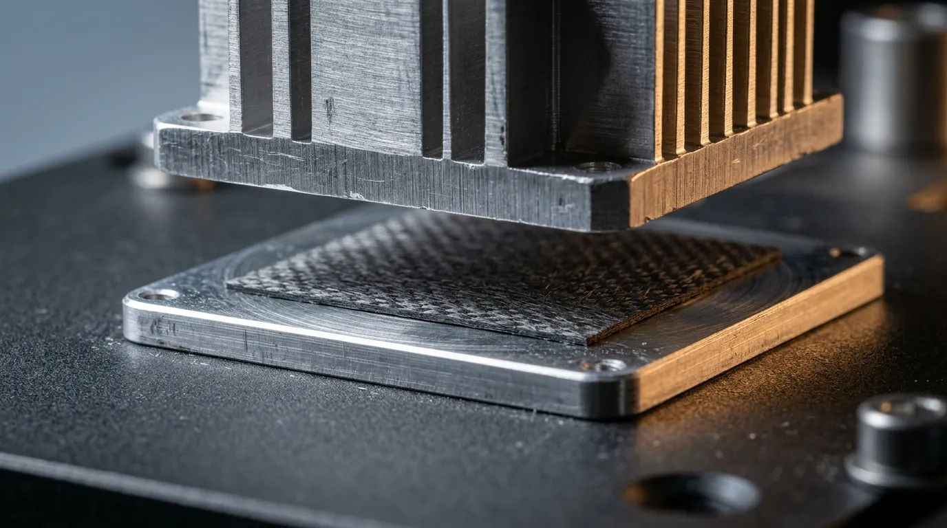
An 800G pluggable carries on the order of 17–18 W into a package whose outside dimensions are fixed by a multi-source agreement, and the few tenths of a millimetre between the DSP lid and the riding heatsink decide how much of that power leaves through the top. That gap is where the optical module thermal interface material decision actually happens — not in a catalogue of bulk conductivities, but at a bond line of 0.30 mm, under a spring force nobody measured, on surfaces that are flat to a tolerance rather than to a polish.
What changes when the material in that gap is an ultra-thin carbon-fiber TIM instead of a silicone gap pad? Three things improve, two get worse, and one popular argument — that a denser pad stores heat and smooths transients — turns out to be wrong at this thickness.
The Interface Inside a Pluggable Is Not a Gap Pad Problem
Start with the mechanics. A pluggable module slides into a folded sheet-metal cage press-fit to the host board; the cage closes it in on five sides and opens on the top, where a spring-loaded riding heatsink presses down on the module lid. The module slides in and out under that spring a couple of hundred times over its service life, without the interface migrating, shedding or welding itself to the lid.
A 2016 review of pluggable thermal specifications is blunt about the space: nominal air gaps between the module case and the cage, and between the cage and the PCB, run about 0.2 mm to 0.3 mm, and the manufacturing tolerances on those gaps are large relative to their size. An interface material here is not filling a designed cavity; it occupies a space whose thickness is partly an accident of three tolerances stacked on each other.
Two consequences follow. The first is that you do not set the bond line — the hardware does. Whatever thickness you specify, the installed thickness is the gap that the lid, the heatsink base and the spring force produce. A pad specified at 0.30 mm that cannot compress will hold the heatsink off the lid at its high spots; a pad that compresses too easily will bottom out, lose its compliance and take a permanent set.
The second is that the interface sees sliding, not just compression. The module is inserted and extracted across the heatsink contact face. A material with adhesive of its own fights that motion; a material that sheds fibre or filler contaminates the cage and, eventually, the optical port.
The Optical Internetworking Forum addressed the specification side in its thermal interface implementation agreement for pluggable optics modules: it defines how interface thermal resistance to an ideal heatsink is characterised, and recommends tighter finish and flatness tolerances than the form-factor agreements require. As power rose, the interface stopped being a detail left to the module supplier.
How the same constraints play out across base-station radios and the wider 5G picture is covered in the cluster's earlier treatment of 5G and optical module thermal materials; this article stays on the interface itself.

Illustration of the cage, module and riding heatsink arrangement — not a photograph of a specific product.
What an Optical Module Thermal Interface Material Has to Satisfy
Optical module thermal management is, at the port level, an interface problem. An 800G optical module of the QSFP-DD800 generation is projected at 17–18 W for client optics and 20–25 W for line optics, and a published QSFP-DD thermal study puts 400G client transceiver modules at 10–14 W and 400G coherent line modules at 16–20 W, against a 25 W per-port design target. None of those watts gets easier to remove because the package stayed the same size.
Six constraints decide whether a candidate optical module thermal interface material fits, and they do not trade off cleanly.
| Constraint | What it means at 0.3 mm | Failure mode if ignored |
|---|---|---|
| Installed thickness | The gap the hardware produces, not the datasheet value | Heatsink held off the lid, or pad bottomed out |
| Available pressure | Spring force divided by contact area, after tolerances | Real contact area too small; resistance climbs |
| Electrical behaviour | Insulating or not, against the two surfaces it touches | Isolation where none is needed, or conduction where isolation is required |
| Attachment | Whether the pad stays put through insertion and extraction | Migration, tearing, contamination of the cage |
| Mass and stiffness | What the spring has to carry and the lid has to tolerate | Retention problems, bowed lids, uneven contact |
| Cleanliness | Volatiles and particles near open optical surfaces | Irreversible contamination of fibre end-faces and lenses |
Notice what is missing from that table: thermal conductivity as a headline number. It belongs in the calculation, but at 0.30 mm the bulk term is small. For a material at 9 W/m·K, a 0.30 mm bond line contributes about 0.33 °C·cm²/W of bulk resistance; at 25 W/m·K it is about 0.12 °C·cm²/W. The same material at 2.00 mm would contribute 2.22 and 0.80 °C·cm²/W — 6.7 times as much, because bulk resistance scales with the thickness ratio.
At this scale, thickness is the dominant variable, and the contact term on either face is often larger than the bulk term in the middle. The distinction is worth fixing before you compare datasheets; the cluster explains it in thermal resistance versus thermal impedance.
Carbon Fiber Thermal Interface Material: What Changes at 0.3 mm
A carbon fiber thermal interface material is a pad whose conductive phase is carbon fibre oriented so that the fibre axis crosses the bond line. That orientation is the design: a carbon fibre conducts far better along its length than across it, so fibres standing on end give the interface a through-plane path the polymer matrix cannot provide.
The ZIITEK TIR®700 series is the concrete data set for this class, and its figures are worth reading as a group rather than as one number:
| Property | TIR®700 series |
|---|---|
| Thermal conductivity | 9–25 W/m·K |
| Thickness | 0.30–0.50 mm and 1.00–5.00 mm (25 W/m·K grade); 0.75–5.00 mm (9 W/m·K grade) |
| Hardness | 85 or 60 Shore OO (25 W/m·K grade); 65 Shore OO (9 W/m·K grade) |
| Density | 2.1–3.3 g/cm³ |
| Specific heat | 0.70–0.93 J/g·°C |
| Service temperature | −40 to 200 °C |
| Electrical behaviour | Electrically non-insulating |
| Adhesive | None of its own |
Three of those rows change how the interface behaves compared with a silicone gap pad.
The thin band is a design point, not the bottom of a catalogue. ZIITEK's silicone range runs 0.25–12 mm, where 0.25 mm is the exception. A series that offers 0.30–0.50 mm on one grade, 0.75–5.00 mm on the other and 1.00–5.00 mm on both is aimed at an installed gap that is a tolerance stack rather than a design feature — and it is a reminder that an ultra-thin thermal pad and its thicker sibling are not the same part at a different thickness. Hardness, thickness and conductivity move together.
There is no adhesive and no tack. Right for a sliding interface, wrong for a vertical assembly that expects the pad to hold itself in place, and convenient for rework: nothing has to be scraped off a lid.
It is electrically non-insulating. In an optical module that is usually an advantage rather than a hazard, for reasons taken up below — but it is a decision, not a default.
These properties place the series inside the site's wider thermal conductive and EMI absorbing material family, where the electrical and absorption questions get complicated.
Conductivity in this class is quoted to ASTM D5470, the standard test method for thermal transmission properties of thermally conductive electrical insulation materials, and what it produces is a bulk property of a specimen at a stated pressure and bond line. The series figures above are published without either, which is the one condition this table cannot supply — so treat 9–25 W/m·K as a bulk range and ask for the test report at your own bond line and pressure before comparing it with another supplier's number.
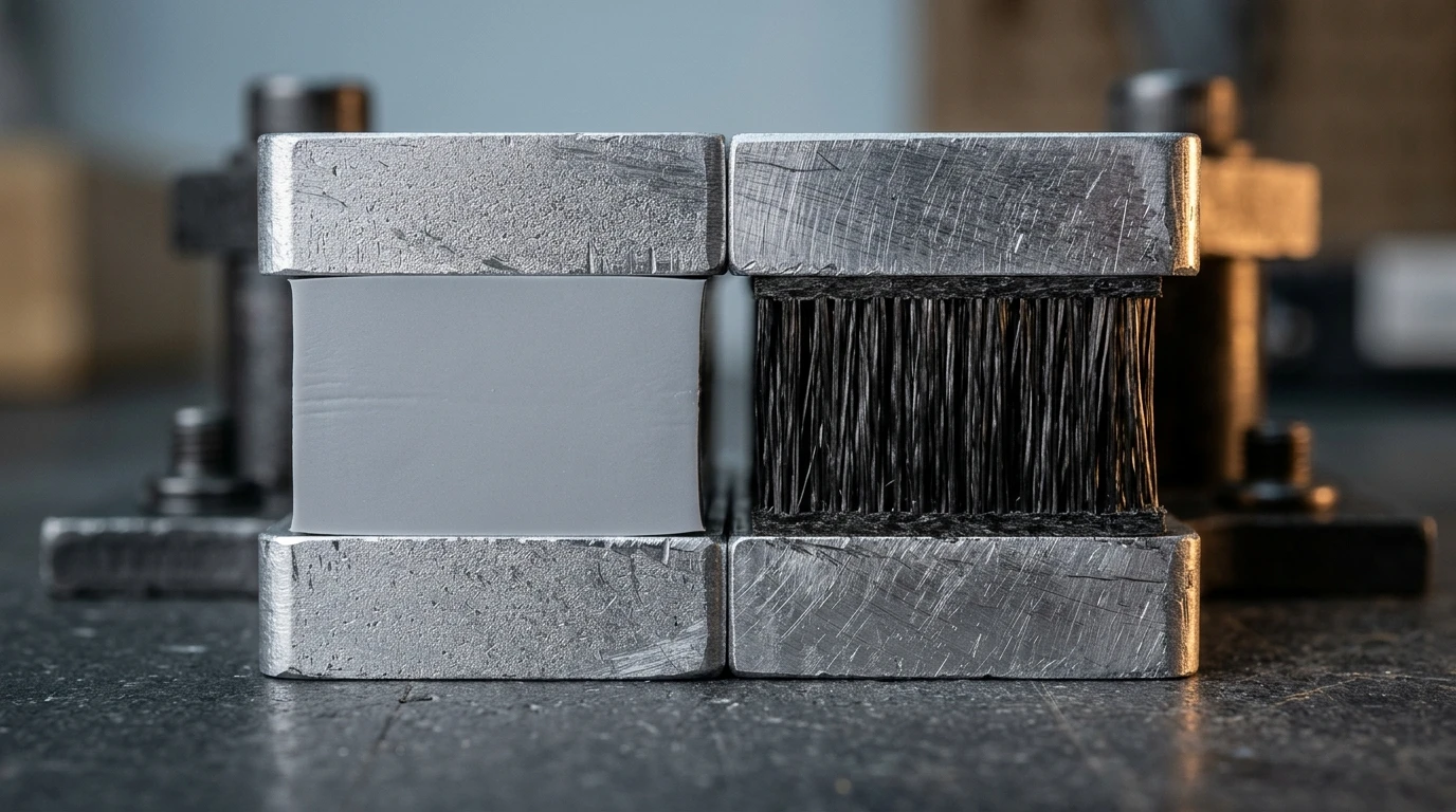
Illustration of the two interface types — not a micrograph of either material.
Thickness, Flatness, and the Bond Line You Actually Get
Flatness is where the arithmetic gets uncomfortable. The same QSFP-DD study records that the current flatness specification in the multi-source agreement, for modules dissipating 10 W and above, is 0.050 mm, and that 0.025 mm would be beneficial for high-power modules if cost allowed.
Put that beside a 0.30 mm pad. The 0.050 mm specifies the module housing surface; the heatsink base carries a second tolerance of the same order, under the system designer's control. One surface alone can put the two faces 0.05 mm further apart at one edge of the contact patch than at the other, and a second tolerance of that size makes the worst case worse rather than equal. If the pad is hard enough that the extra compression is unavailable, the high spots carry the load and the rest of the interface is an air gap — and air conducts two orders of magnitude below the pad, so a contact gap is a different regime, not a small penalty.
This is the trade a thin carbon-fiber pad makes: the thin band keeps the bulk term small, but leaves less absolute material to spend on flatness error. At 0.30 mm every micron matters, and softness rather than conductivity becomes the binding constraint.
The compression that closes the error has to come out of a documented part of the pad's thickness. At 0.30 mm nominal, a 0.05 mm error is already a sixth of the pad, so the question is not whether the material is soft but what deflection it takes at your pressure without bottoming out — ask for the compression curve before assuming a third of the thickness is available. If the design can hold 0.025 mm flatness, the same pad has twice the margin.
Bond line thickness and compression allowance are worked through in the pad thickness and compression guide; the optical-module addition is that the flatness allowance comes from the form factor, not from a machinist.
Contact at Low Mounting Pressure
Pressure is the variable engineers most often assume and least often measure. In a pluggable, normal force comes from the riding heatsink spring, transmitted through the cage opening onto the module lid, and several things cap it: the module has to slide in and out, the latch has to be operable by hand, and the housing has to survive the load without deflecting into the optical sub-assembly. The result is a pressure that is modest, variable with module height, and rarely stated as a number in the form-factor agreement — the same review notes that some agreements specify allowable contact forces and some do not, and that surface finish and flatness were historically set for manufacturability rather than thermal control.
At low pressure, hardness becomes a first-order property. A pad at 85 Shore OO needs more normal force than one at 65 Shore OO to reach the same real contact area (lower Shore OO is the softer material), because it resists the local deformation that lets it follow surface texture. The grade structure has a consequence that is easy to miss: in the TIR®700 range the 65 Shore OO grade is the 9 W/m·K material, supplied from 0.75 mm upward, while the 0.30 mm band belongs to the 25 W/m·K grade at 85 or 60 Shore OO. The series' softest grade is 60 Shore OO, and the 65 Shore OO 9 W/m·K grade starts at 0.75 mm — so below 0.75 mm there is nothing softer to step down to. A weak spring over a 0.3 mm gap is therefore not something this series solves by going softer. It is a signal that the interface needs a different material family, or a design change that lets the spring do its job.
Paste deserves the same honesty: at its installed bond line — a film a fraction of the 0.3 mm gap — a dispensed grease has lower bulk resistance than any pad, and a pad will not beat it on that number. What paste cannot do is hold a bond line — its thickness is whatever dispense volume and clamp force leave behind, and under a lid that slides it has no defence against pump-out. That is why pads, not pastes, are the default here.
If the pressure range is very low or very uneven, a pad may be the wrong form factor altogether and a gap filler, thermal gel or phase-change film fits better; the trade-offs are in gap filler versus gap pad versus phase change material.
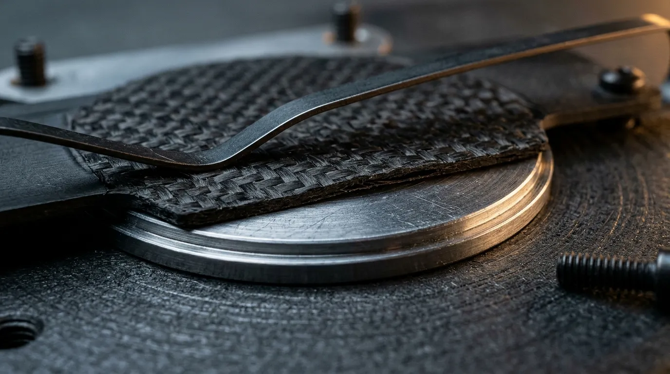
Illustration of partial contact under light spring load — the uneven gap is exaggerated for legibility.
Non-Insulating Contact on a Metal Cavity
Most thermal interface guidance treats electrical insulation as a virtue. In a pluggable optical module it is often just extra thermal resistance, and sometimes a requirement that does not exist.
Follow the surfaces. The pad typically sits between the module lid — a metal housing that also provides the mechanical and EMC enclosure — and the heatsink base, which is bonded to the chassis. Both faces are metal, and both sit at the same potential whenever the module housing is grounded through the cage: the usual arrangement, but one the designer should confirm rather than assume. In that geometry a pad that does not insulate is not a hazard; it is one less layer between metals already in contact through the enclosure.
Where it matters is everywhere else. A non-insulating pad must not bridge a live trace to a grounded surface, must not substitute for a grounding conductor, and must not be relied on to isolate a floating node. It is also not specified as an electrical contact material: "not an insulator" and "a good conductor" are different claims, and this class of pad supports the first, not the second.
| Interface between | Non-insulating pad | What to check |
|---|---|---|
| Module lid and heatsink base, both grounded to chassis | Acceptable | Continuity already exists; confirm nothing live passes under the pad |
| Live trace, pad, grounded housing | Not acceptable | Requires a stated breakdown voltage, not a conductivity figure |
| Floating node, pad, chassis | Not acceptable | Isolation is a safety function here; specify it as one |
| Two faces at different potentials within the module | Not acceptable | Resolve the potential difference before choosing a TIM |
The decision is therefore a question about the two surfaces, answered before the thermal one. If both faces are the same grounded metal, conduction through the interface removes a dielectric layer and usually improves wetting against the machined lid and the copper or aluminium heatsink base. If either face carries a potential, the interface needs an insulating material; the options and their breakdown ratings are covered in thermally conductive electrical insulators.
Mass, Density, and a Millisecond Answer
Density is the property most often sold and least often needed. The TIR®700 series runs 2.1–3.3 g/cm³. Take a contact patch of 20 × 20 mm at 0.30 mm: 0.12 cm³, so the pad weighs 0.25–0.40 g. Against a cage spring holding a module in place, that is not a retention problem and not a reason to choose one material over another; the lightweight argument earns its place in large-area or stacked assemblies.
The related claim — that a denser pad stores heat and buffers transients — is worth checking with numbers.
Thermal diffusivity is conductivity divided by density times specific heat. For the 25 W/m·K, 2.9 g/cm³, 0.75 J/g·°C grade it is about 1.1 × 10⁻⁵ m²/s; for the 9 W/m·K, 2.1 g/cm³, 0.93 J/g·°C grade, supplied from 0.75 mm upward, about 4.6 × 10⁻⁶ m²/s. A heat-flux step takes roughly L² divided by diffusivity to cross a layer of thickness L, so at 0.30 mm the 25 W/m·K grade crosses in about 8 ms; the lower-conductivity grade would take about 20 ms at that thickness, and about 120 ms at its actual 0.75 mm minimum. Thickness, again, does more of the work than conductivity.
The interface responds in milliseconds, not seconds. Its volumetric heat capacity is 1.95–2.31 J/(cm³·K), so a 0.12 cm³ pad holds roughly 0.25 J/K — a 17 W module shifts its temperature by 1 K in about 15 ms. It is a resistor with a negligible thermal mass, not a heat buffer, and choosing a denser material for its "thermal inertia" is choosing mass you do not need.
When Carbon Fiber Is the Wrong Choice
A material-led article that does not disqualify its own material is a sales page. Six conditions point away from an ultra-thin carbon-fiber pad, and one points away from pads in this format generally.
| Condition | Why carbon fiber loses | Direction instead |
|---|---|---|
| Installed gap above about 0.5 mm, or strongly uneven | The thin band is the design point; the thicker grade exists, but the thin-pad advantage disappears | Dispensable gap filler, or a phase-change film that flows at operating temperature |
| Either face carries a potential | The material is electrically non-insulating by design | An insulating pad with a stated breakdown voltage; boron-nitride-filled grades exist for low-dielectric joints |
| The pad must hold itself in place during vertical assembly | No adhesive, no tack | A tacky gap pad, or a mechanical retainer |
| An open fibre end-face, lens or laser window is nearby and low volatility is required | Low-volatility performance is a separate specification, not a property this series is sold on | A low-volatile silicone pad, or a non-silicone pad where silicone is excluded outright |
| The hotspot problem is lateral, not through-plane | A through-plane pad moves heat across the bond line, not along the lid | A graphite spreader, which spreads in-plane |
| The gap is flat, the clamp is controlled, and nothing slides across it | A thin pad is close to paste on bulk resistance, not below it | Paste or thermal grease, where clamp force sets thickness and there is no pump-out path |
| Module power is low and cost dominates | The thin-pad premium buys nothing at 3 W | A standard silicone gap pad |
The fourth row is the one that gets skipped. Optical modules put an interface within millimetres of open optical surfaces, and molecular contamination of a fibre end-face is not field-serviceable. Volatility has its own test methods and is not implied by conductivity, hardness or thickness. The test data and its limits are covered in reading ASTM E595 low-outgassing data for thermal pads; a low-volatile silicone grade and a non-silicone grade are the two families that answer it, and both are specified separately from the carbon-fiber series.
Rework is the other limit: a pad without adhesive lifts cleanly, but one run at the compression limit of its curve and cycled to 200 °C should not be reused. Plan the interface as a replaceable part with a defined compression allowance.
A Selection Sequence for a 0.3 mm Interface
Put the sections together and the sequence runs on a real design in an afternoon.
- Measure the gap, not the drawing. Stack the lid, the heatsink base and the module height tolerance, and take the worst case at both ends of the contact patch. If the range crosses 0.5 mm, a pad is the wrong family.
- Measure the force. Spring rate at installed height, on a real cage, divided by the contact patch. It is the input most selections skip.
- Decide the electrical question first. Same grounded metal on both faces allows a non-insulating material; any potential difference requires an insulating one, and that overrides the thermal preference.
- Choose hardness for the pressure, then conductivity for the flux. A pad that cannot deform to the surface texture will not make contact, whatever its datasheet conductivity.
- Verify at the low end of the pressure range. A test at nominal force tells you what the design can do; a test at minimum force tells you what the product will do in the field.
For a 0.30–0.50 mm interface between a grounded metal lid and a metal heatsink base, with a spring delivering a few newtons over a few hundred square millimetres, the shape of the answer is an ultra-thin, adhesive-free, non-insulating carbon fiber TIM sized to the flatness budget — in the TIR®700 range that means the 25 W/m·K grade — 85 or 60 Shore OO, whichever hardness its datasheet pairs with your thickness band — since the 65 Shore OO 9 W/m·K grade only starts at 0.75 mm. That is the whole decision at this thickness: two measured numbers and one electrical question. If your interface has different constraints, send the stack-up and the measured force to our application engineers — the material choice usually follows from those two numbers, not from a conductivity table.