EMI Shielding Basics for Electronics Engineers
EMI shielding for electronics is a choice of reflection or absorption, not a metal wall. Learn the mechanisms, board-level moves and specs that decide a fix.
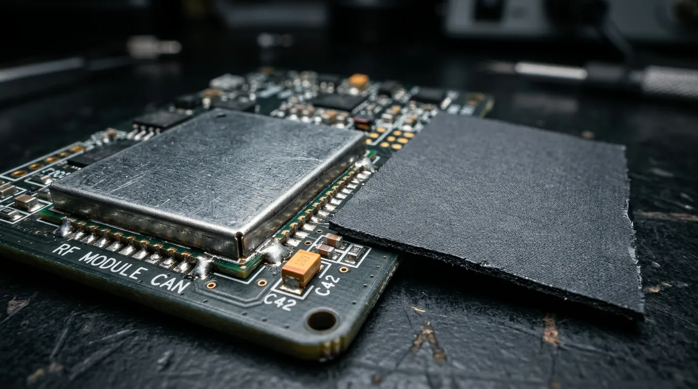
A radiated-emissions test fails at 2.4 GHz two days before a build freeze. A shield can that was supposed to quiet a power supply starts ringing at a harmonic instead. Two high-speed lanes couple into each other and the eye closes. The reflex in every case is the same — add metal, close the box — and in a surprising number of those cases the metal is what is making the problem worse.
EMI shielding for electronics is not the act of wrapping a board in a conductor. It is the act of deciding which physical mechanism removes or redirects a specific noise, at a specific distance, on a specific layer of the product. Get the mechanism right and a 0.1 mm absorber sheet fixes a problem that a metal enclosure only relocated. Get it wrong and you spend a week adding shielding that turns a radiating trace into a resonating cavity.
This guide is written for the engineer holding the board, not the one specifying the chassis. It works through what shielding actually does, why reflection and absorption are not interchangeable, where the noise sits relative to the source, and which moves solve most problems at board level — then how to read a shielding-effectiveness number and what to test.
What EMI Shielding for Electronics Actually Does
Electromagnetic interference is energy from one circuit that corrupts another. A switching node, a clock, a radio, a cable or a motor drive emits a changing electric and magnetic field; a nearby trace, sensor or receiver picks it up and sees a signal that was never sent. Shielding is any conductive or magnetic barrier placed between the two, and it works by attenuating the coupling path rather than by blocking it outright.
That distinction matters more than it sounds. No practical shield reduces a field to zero. It reduces it by a factor, and the factor is what you design to — measured in decibels of shielding effectiveness. Because decibels are logarithmic in field strength, the scale is easy to underestimate: 20 dB is a tenfold reduction, 40 dB is a hundredfold, and 60 dB is a thousandfold. A part quoted at "60 dB" and a part quoted at "80 dB" are not 33% apart; the second leaks one-tenth as much field as the first.
The classic mental model is the Faraday cage: a conductive enclosure that keeps external fields out and internal fields in. It is a useful picture and an incomplete one. A perfect, seamless, closed conductor would shield almost ideally. Real enclosures have seams, ventilation slots, connector cut-outs and cable penetrations, and those features — not the metal — set the real performance. A welded steel box and a plastic housing with a sprayed conductive coating can end up in the same range once the apertures are counted, which is why "just use metal" is not a design answer. The physics of the enclosure is summarised in the standard reference on electromagnetic shielding, and the reason any of it is mandatory in the first place is regulation: in the United States, 47 CFR Part 15 sets the radiated-emission limits that unintentional radiators — which is to say most digital electronics — must meet before they can be sold.
So the real question is never "shield or not." It is which mechanism, at which layer, and how much. One piece of vocabulary is worth fixing first, because engineers are asked it constantly: EMI is the phenomenon — unwanted energy coupling from one circuit to another — while EMC is the compliance state a product has to demonstrate, covering both what it emits and what it tolerates. Shielding is one lever on the emissions side of EMC; filtering, grounding, layout and cable treatment are others, and a design that only shields is rarely a compliant one.
Reflection vs Absorption: The Choice That Decides the Fix
Shielding works through two mechanisms that behave very differently, and confusing them is the most common and most expensive selection error in this space.
Reflection happens at the surface of a conductive barrier. The wave meets a boundary between air and a material whose impedance is far lower, and most of its energy bounces back. Copper, aluminium, steel foil, shield cans, conductive coatings and conductive fabric all work primarily this way. Reflection is cheap, broadband, and effective — the reason metal became the default. Its weakness is exactly what makes it cheap: the energy is not removed, it is redirected. A metal can around a noisy source traps that energy inside, and if the cavity has dimensions that resonate at a harmonic of the noise, the enclosure becomes an antenna and radiates more efficiently than the bare board did.
Absorption happens inside a lossy material. Soft-magnetic particles — ferrite-type fillers — flip their magnetic domains under the passing field, and that motion dissipates the wave's energy as heat instead of returning it. An absorber sheet is typically a thin, flexible, dark composite that you place next to the source, not around it. Because the energy leaves the system as heat rather than bouncing, absorption is the right tool when the problem is a resonance, a ground-plane bounce, a noisy heat sink, or a surface current on a shielded enclosure. An industry explainer on how EMI absorbers work lists the iron, nickel and zinc oxide filler mixtures used in soft-magnetic absorbers.
The practical rule that falls out of this: reflect when you need a wall, absorb when you need to kill a resonance. Most mature designs use both — a can for containment, an absorber inside it to damp the cavity it creates.
There is a second reason to think in terms of absorption, and it belongs to this site's material family. An absorber is a filled composite, and the same filler network that dissipates RF energy can be engineered to conduct heat. That is the origin of the two-in-one class covered in our thermal conductive + EMI absorbing materials overview: one pad that damps a shield-cavity resonance and moves heat out of the component underneath it at the same time. Whether that is the right part for your board depends on the next two questions — where the noise is, and how hot the source runs.
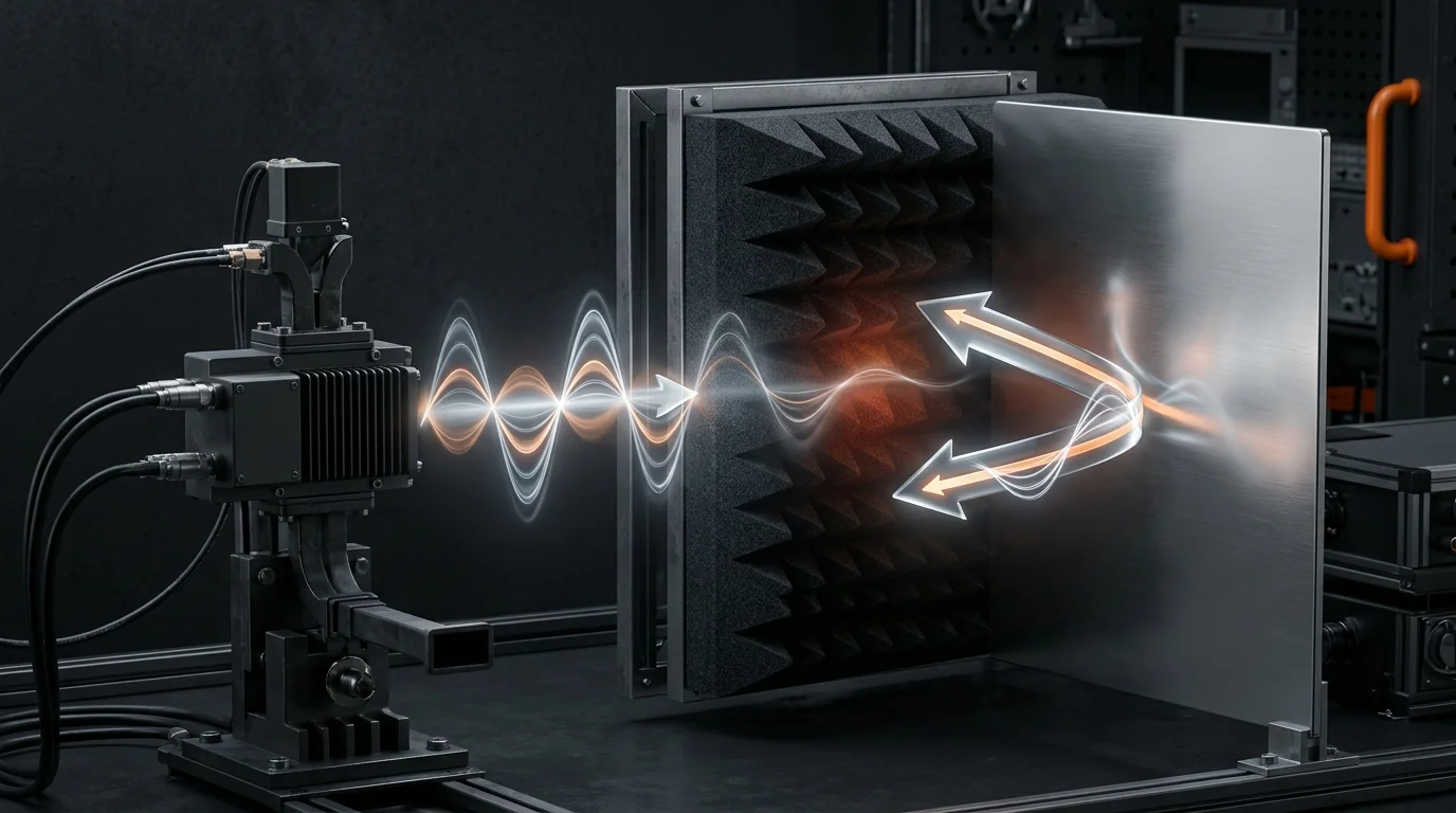
Reflection returns the energy to the cavity; absorption removes it. Which one you want depends on whether the problem is a field to contain or a resonance to damp.
Near-Field vs Far-Field: Which Mechanism Fits
Distance from the source changes which part of the field dominates, and that decides which mechanism and which material thickness will do any good. Engineers who skip this step often buy the right material for the wrong field.
Close to a source — within roughly a wavelength divided by 2π — the field is in the near field. Here the electric and magnetic components are not yet in a fixed ratio; one or the other dominates depending on whether the source is a high-current loop or a high-voltage node. A switching power supply with a tight current loop is a predominantly magnetic source, and a magnetic near field is best dealt with by a material with high magnetic permeability — a ferrite-type absorber — not by a thin conductive foil, which reflects poorly at low impedance. At 1 GHz the near-field boundary sits at about 48 mm; at 2.4 GHz, about 20 mm. On a crowded board, that is exactly the scale at which neighbouring components live. The technical definition of the near-to-far transition is summarised in the reference on near and far field.
Beyond that boundary — the far field — the wave has settled into a plane wave with a fixed ratio between its electric and magnetic components. Here a conductive barrier reflects efficiently, and thin metal, mesh or conductive coating works well, because the energy is largely electric-field coupled and a conductor of even a few skin depths is enough. This is the regime in which enclosure-level shielding and cable shielding operate.
| Near field (source-adjacent) | Far field (radiated) | |
|---|---|---|
| Distance from source | Less than ~λ/2π | Greater than ~λ/2π |
| Dominant field | Magnetic (loops) or electric (high-impedance nodes) | Plane wave, fixed E/H ratio |
| Best mechanism | Absorption (high-permeability filler) | Reflection (conductive barrier) |
| Typical fix | Thin absorber sheet at the source | Shield can, foil, mesh, conductive coating |
| Material thickness | Set by absorption band, often 0.03–2.0 mm | A few skin depths of the conductor |
The takeaway is mechanical: if your noise problem is a hot loop on the board, a metal can bolted over it reflects poorly and traps what it catches. Put an absorber where the field is still magnetic and let it turn the energy into heat.
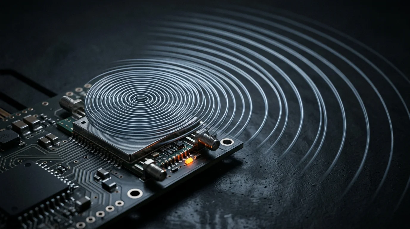
Wavefronts spreading from a source on a board: the field close to the source and the field far from it behave differently, which is why the mechanism has to match the distance.
Board-Level Shielding: Three Moves That Solve Most PCB Problems
Most of the shielding advice available online is written for the enclosure. Most of the failures are on the board. At board level, three moves cover the large majority of real cases, and they are complementary rather than alternative.
1. Contain a component in a shield can. A metal can soldered or clipped over a radio, a switching regulator or a clock source is the blunt instrument of board-level shielding, and it is often the right first move. Its performance is decided almost entirely by how it is grounded: a can bonded at many points along its perimeter behaves like a wall, while one grounded at a couple of tabs behaves like a patch antenna with a deliberate resonator inside. The can also creates the cavity-resonance risk described above — which is why the next two moves usually accompany it.
2. Close the seams with a conductive gasket. The can's own perimeter, the connector shells, and the gap between a module and its host are all potential leak paths. A conductive elastomer gasket — a particle-filled silicone that is electrically conductive as well as compressive — bridges that gap and keeps the seam continuous. This is where mechanical and electrical requirements meet: the gasket must compress enough to close the electrical path and seal environmentally, but not so much that it crushes the connector or fatigues over thermal cycles. For a powered module there is a thermal question underneath the same seam, and the trade-off between gap-filling formats — compressible pad versus dispensable gel versus phase-change sheet — is worked through in our comparison of gap filler, gap pad and phase-change materials.
Selecting on thermal impedance at the assembly's real pressure, rather than on a headline conductivity number, is described in thermal resistance versus thermal impedance.
3. Absorb at the source. Absorber sheets go where the noise starts: on top of the offending component, on the inside of the can lid, along a flex cable that carries a fast edge, or on the heat sink that has become an unintentional radiator. Thin and light, they add almost nothing to the stack height and damp the energy before it couples to the enclosure. This is the move that most often turns a failing pre-compliance scan into a passing one, and it is the move that is missing from most published EMI explainers.
| Move | Mechanism | Solves | Limit |
|---|---|---|---|
| Shield can over the component | Reflection | Radiated emission from a known source; also engine of cavity resonance | Needs many ground points; can resonate |
| Conductive gasket at seams | Reflection, continuity | Leakage at enclosure seams, connectors, module interfaces | Compression must match the hardware |
| Absorber sheet at the source | Absorption | Cavity resonance, surface currents, near-field coupling, cable noise | Tuned to a frequency band; adds a thermal path to size |
Put in order, that sequence also matches how most boards are actually fixed: contain, seal, then damp — and go back to the absorber first when the first two moves leave a residual peak in the scan.
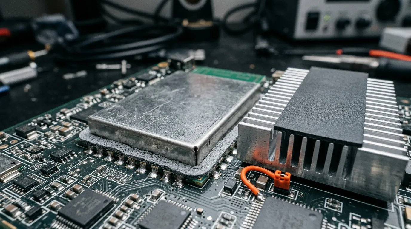
The three board-level moves are complementary: the can contains, the gasket closes the seam, and the absorber damps what the can would otherwise trap.
The Materials Map: From Copper Foil to Conductive Elastomer
Shielding materials differ far more in the format they suit than in how "good" they are. Sorting them by role is more useful than sorting by conductivity.
- Metal foil, mesh and screen. The classic reflectors. Copper and aluminium foil are the cheapest way to line a housing; metal mesh trades conductivity for ventilation and weight; expanded metal foil covers irregular surfaces. All reflect, and none absorb — they are the right answer in the far field and the wrong one for a cavity that is already resonating.
- Conductive coatings and paints. Silver-, nickel- or graphite-filled paints apply shielding to plastic enclosures that would otherwise be transparent to RF. They make injection-moulded housings behave like shielded ones at low weight, and they wear or flake at high-wear points such as connector openings.
- Conductive plastics and polymers. Carbon- or metal-filled polymers mould directly into a shielded part, which is attractive for high-volume enclosures and for parts that need shielding and structural function in one shot.
- Conductive gaskets and elastomers. Particle-filled silicones that seal and conduct in the same part. They are the standard answer at seams and module interfaces because they solve the mechanical and electrical problems together.
- Thermally conductive insulators. For joints that must pass heat while blocking current — the MOSFET-to-heatsink interface in a power stage, for example — a dielectric sheet does the shielding-adjacent job. ZIITEK's thermally conductive insulator family sits in the 1.0–1.6 W/mK range with dielectric strength in the 1,500–6,000 VAC class; the thermal conductive insulators guide explains where they belong.
- Absorbers and combined thermal + absorber materials. The class that removes energy rather than reflecting it, and the class that can be engineered to conduct heat as well. The distinction between a pure absorber and a combined pad — and how each is specified across a frequency band — is the subject of our two-in-one thermal conductive + EMI absorbing materials guide.
Two properties separate materials within the absorber class, and both live in the datasheet's fine print. Initial permeability describes how strongly the magnetic filler responds to a field, and it sets how well a thin sheet absorbs in the low megahertz to low gigahertz range. Frequency band is the range over which the part actually attenuates; an absorber is tuned, not broadband magic, and a pad that works at 10 MHz may do nothing at 10 GHz. A sheet is not fully specified until both numbers are on the table.
Reading a Shielding-Effectiveness Spec
Once a material or enclosure claims a shielding-effectiveness figure, the engineering question is what that number was measured at and whether it survives your seams.
Shielding effectiveness is the ratio of field strength without the barrier to field strength with it, expressed in decibels. Because it is measured against a specific test setup and frequency, a bare "60 dB" means little until you know the method. The two names you will meet at enclosure level are MIL-STD-285 — the classic military method, cancelled in 1997 — and IEEE 299, which replaced it; both specify how to launch a field, where to measure it, and over what frequency range — so two suppliers quoting "60 dB" against different methods may not be comparable at all. For material-level measurements, the picture narrows further to the specific fixture and frequency band of the datasheet.
The number that actually matters on your board, however, is usually not the material's — it is the assembly's, and apertures dominate it. Every opening in a conductive barrier is a slot antenna, and as a rule of thumb an aperture starts to leak once its longest dimension approaches a meaningful fraction of the wavelength you are trying to contain — commonly cited as roughly one-twentieth. At 1 GHz, with a wavelength of about 300 mm, that puts the limit near 15 mm; at 10 GHz, with a wavelength of 30 mm, it is closer to 1.5 mm. A single unfastened screw, a connector with a painted flange, or a lid bonded at too few points can quietly become the limiting feature of an otherwise excellent shield. This is why the practical specification for a shielded assembly always includes the grounding and gasket details, not just the metal.
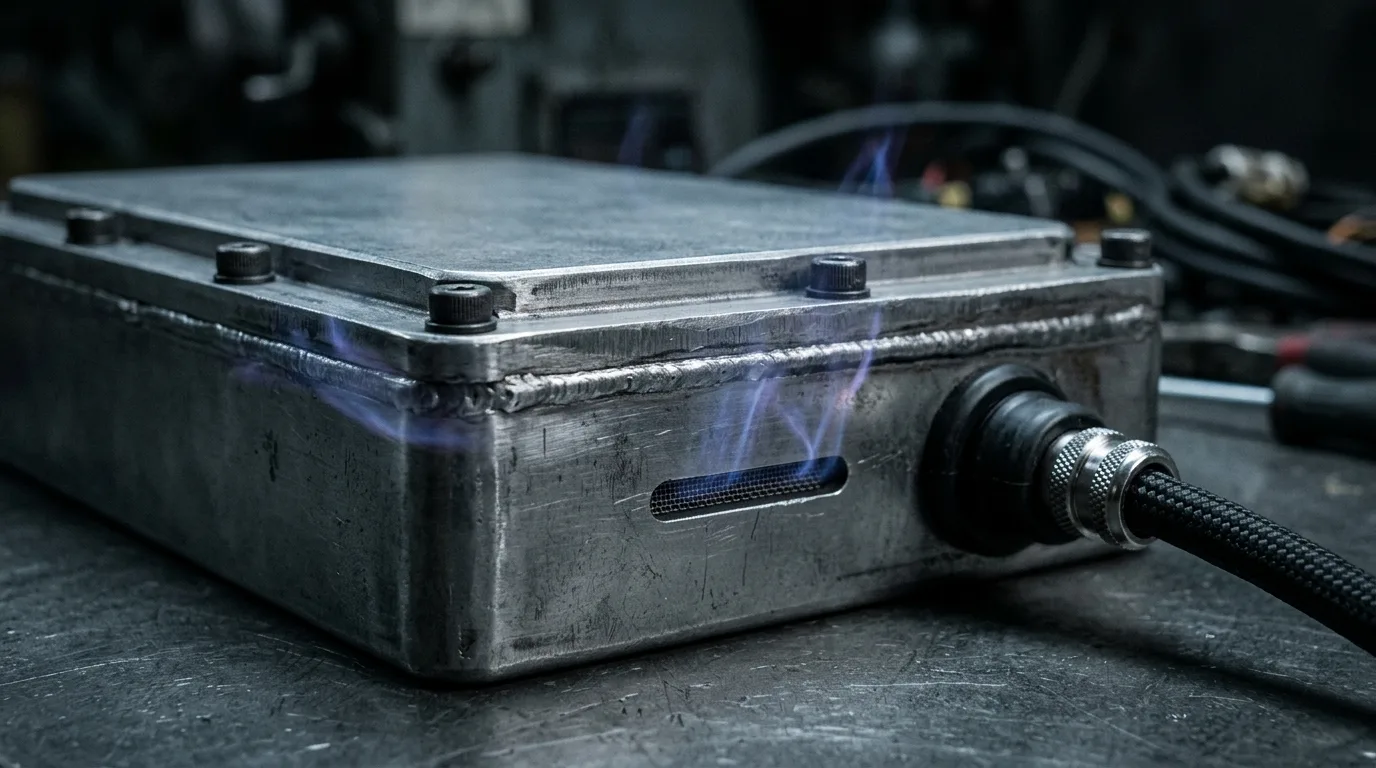
On a real enclosure the seams, slots and cable penetrations — not the metal — set the shielding effectiveness you actually get.
Two compliance threads run alongside the electrical performance. Flammability is one: enclosures, gaskets and internal materials in consumer and industrial electronics are routinely required to meet a UL 94 rating, and the difference between the solid-material rating and the thin-film rating matters when your interface is a 0.1 mm sheet rather than a 2 mm pad — the distinction our UL 94 V-0 versus VTM-0 comparison works through, based on the combustion tests for plastics themselves. Substance compliance is the other: for anything shipping into Europe, RoHS and REACH documentation is not optional. Industry does not apply those requirements evenly, either — medical, aerospace and military assemblies typically carry the tightest shielding and documentation requirements of all, which is why in those sectors the test method and the aperture budget get pinned down before the material is chosen.
When the Noisy Part Is Also Hot
The two problems this guide has treated separately — noise and heat — usually arrive in the same place. The components that radiate are the components that burn power: a 5G power amplifier, a high-speed DSP, a switching regulator, a GPU under load. That coincidence is why the two-in-one material class exists, and why it is worth understanding as a category rather than as a curiosity.
A combined thermal and absorbing material is a single filled sheet that does both jobs. One filler network conducts heat into the heat sink; a soft-magnetic filler dissipates RF energy as heat rather than reflecting it. Placed between a hot, noisy component and its heat sink, the pad replaces what would otherwise be two parts — a thermal interface material and a separate absorber — plus the tolerance stack and assembly step that come with a second layer. On a densely packed RF board with dozens of interfaces, removing one part per hot spot is a manufacturing advantage as much as a thermal design choice.
ZIITEK supplies this class at two ends of the family: a combined thermal-and-absorbing pad, and a dedicated absorber. The TIF®900 series is a thermally conductive and wave-absorbing material formulated for 5G antennas, base stations, optical modules and mmWave radar, spanning roughly 1.5–4.0 W/mK with halogen-free, lead-free construction. The TIR®900 series is a dedicated absorber line covering the 10 MHz to 18 GHz range in three tuned classes, with initial permeability in the 30–200 range and thicknesses from 0.03 mm up to 2.0 mm; it is used to quiet shielded cavities, damp noise on flex cables and reduce surface currents. Both are supplied as die-cut parts, which is worth planning for early: the accuracy of a die-cut pad is part of the thermal result, and a pad placed imprecisely fails like a wrong one. The converting process behind those tolerance-controlled shapes is explained in what skiving is and how precision converting works.
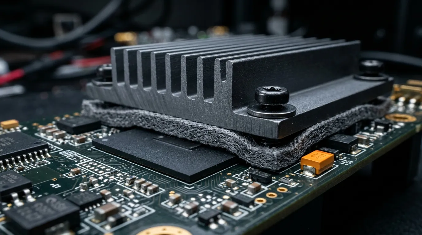
One filled sheet, two jobs: the same composite that conducts heat into the sink absorbs RF energy instead of reflecting it.
What to Test, and How to Choose
Testing closes the loop, and the order of testing matters as much as the equipment. The affordable sequence is a pre-compliance scan of the bare board, a scan with the shield can and gasket in place, and a scan with the absorber added — each step tells you which move did the work, so you can remove the ones that did not. Full certification then follows the applicable standard: IEEE 299 — which superseded the cancelled MIL-STD-285 — for enclosure-level shielding effectiveness, and the radiated-emission limits of FCC Part 15 or the equivalent regime for the market you ship into. When the assembly is a safety-relevant product, the underlying safety standard for audio/video and ICT equipment, IEC 62368-1, usually governs as well.
When you take the problem to a supplier, a short list of questions separates a material that will work from a datasheet that merely looks good:
- Which mechanism is this material — reflective or absorptive — and across what frequency band?
- What is the initial permeability, and how does the absorption band shift with thickness?
- At my mounting pressure and bond line, what is the thermal impedance? A W/mK figure alone does not predict your interface.
- What are the UL 94 and RoHS/REACH documents, for the market I ship into?
- Can you die-cut to my geometry, and what tolerance can you hold?
That last question is not a procurement detail. A correctly chosen material placed imprecisely fails like a wrong one, and dielectric and mechanical tolerances are where board-level shielding projects most often lose their timing.
If the same component is both your noise source and your hot spot, the combined thermal and wave-absorbing pads are specified in our thermal material range to do both jobs at one interface — send us the geometry and the frequency band you need to contain, and we will tell you whether a single sheet will do it.
The engineer's version of EMI shielding is small and specific. It is not a metal box; it is a decision about mechanism, distance and layer, made early enough that the fix is a 0.1 mm sheet rather than a chassis redesign. Get those three right and the failing scan is usually an afternoon's work, not a project.