RF Absorber Selection Guide: Applications & Specs
An RF absorber is a tuned part, not a broadband wall. See the five application families, why their dB numbers differ, and the checks to run before you commit.
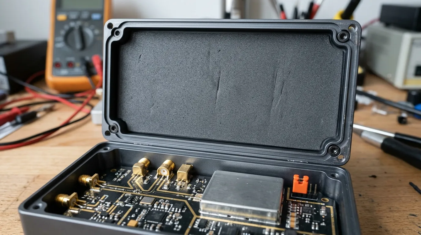
A radio passes its radiated-emissions scan with the lid off and fails it with the lid on. A receive antenna that met isolation on the breadboard loses margin once a metal bracket moves next to it. In both cases the reflex is identical — add shielding — and in both cases the shielding is what changed the problem, because a closed metal box around a radiating board is a resonant cavity, and a cavity re-radiates at the frequencies it prefers. More metal is the wrong medicine here; an RF absorber is the right one.
An absorber removes that energy instead of bouncing it around, but "absorber" is not a specification. A 0.5 mm sheet tuned to 3 GHz acts far closer to a reflector at 300 MHz, and a conductive foam that quiets a cabinet can short a trace it touches. This guide works through where absorbers are actually used, which numbers on the datasheet decide the outcome, and how to prove the part works on your own board before it reaches a build.
What RF and Microwave Absorbers Actually Do
An RF absorber is a lossy composite — soft-magnetic or dielectric filler dispersed in a silicone, elastomer or foam matrix — that lets an electromagnetic wave enter and converts its energy into heat inside the material instead of reflecting it back into the enclosure. The filler does the work; the matrix is chosen for temperature, flexibility and how the part is mounted. No single name covers the family: catalogs list RF absorbers, microwave absorbers, RF microwave absorbers and EMI absorbers side by side, and signature-control suppliers call one class of the same sheet a radar absorbing material. The questions to ask about any of them are identical, so this guide uses the terms interchangeably.
Two loss mechanisms dominate. Magnetic loss comes from ferrite-type fillers whose domains flip under the passing field; these materials are dense, and their high permeability lets a thin layer do work at lower frequencies. Dielectric loss comes from carbon or graphite loading in a foam or elastomer; a microwave absorbing material built this way is lighter and cheaper, but its conductivity makes it unsuitable in direct contact with circuitry. Which mechanism you want depends entirely on the application, and the difference shows up in the next section.
The distinction from shielding matters more than any single number. A shield reflects; an EMI absorber dissipates. Shields are still how most products meet the radiated-emission limits of FCC Part 15, and the mechanisms are compared in our EMI shielding basics for electronics engineers. What an absorber adds is a way to remove energy that a shield would otherwise trap, reflect, or convert into a standing wave.
There is also a second axis nobody puts on page one: free space versus enclosed space. In free space the absorber has to present an impedance close to 377 Ω to the incoming wave and is judged on how much reflection it removes. Inside an enclosure there are no propagating waves at all — only standing waves with the electric and magnetic fields 90° out of phase — and material resonance is no longer the design goal. The transition is not a hard line: field maps published by absorber manufacturers show cavity behaviour breaking down once the enclosure is roughly five wavelengths across, which at millimetre-wave frequencies can be less than an inch. The same box is a cavity at 6 GHz and quasi-free-space at 60 GHz, which is why a part that works in one product can do nothing in a superficially similar one.
That is also why the RF absorber family splits into two commercial types. Reflectivity absorbers are specified against a metal plate: the number is how much less energy comes back. Insertion loss absorbers are specified between two points: the number is how much signal is lost travelling from A to B. Both are legitimate, and they are not interchangeable. If you are choosing a part for a noisy board rather than lining a chamber, note that covering the whole 10 MHz–18 GHz range takes three tuned classes rather than one; the thermal-conductive side of the same material family is covered in our thermal conductive + EMI absorbing materials hub.
Five Application Families Where Absorbers Earn Their Cost
Absorbers are sold as a material and bought as a fix. The applications below cover almost every board-level case, and each one implies a different set of parameters.
| Application family | What actually goes wrong | Usual absorber form | Band priority |
|---|---|---|---|
| Enclosure and cavity resonance | Metal lid turns the board into a resonant cavity; emissions spike at cavity modes | Magnetic elastomer sheet or tile, bonded to lid and walls | 1–18 GHz, plus the low band for small cavities |
| Antenna isolation and pattern control | Coupling between Tx and Rx, surface currents on the ground plane, radome reflections raising sidelobes | Thin sheet between radiators, absorbers in radome tips and antenna hats | Matches the antenna's own band |
| Board-level near-field suppression | Heat sink, connector or flex acting as an unintentional antenna a few millimetres from a victim | Thin, low-conductivity sheet placed on or beside the radiator | 500 MHz–6 GHz typical |
| Millimetre-wave modules and radar | 24, 60 and 77 GHz modules where the package is several wavelengths across | Thin dielectric absorber, 18–40 GHz class | 18–40 GHz and above |
| Test environments and instrumentation | Chamber and test-box reflections corrupting measurements | Pyramidal or wedge foam, hybrid ferrite-plus-foam | 30 MHz–40 GHz |
The first family is where most redesign money is spent, and it is covered in detail below. The second is the one buyers most often get wrong, because isolation is easy to measure and hard to attribute.
For 5G radios and optical modules, absorbers rarely work alone — the same module that radiates also runs hot, and the thermal side of that stack has its own selection logic in our guide to thermal materials for 5G base stations and optical modules. Handheld and wearable products add a third requirement: absorbed energy and nearby radiating elements both raise exposure, and the limits that apply are the ones the FCC sets for radio-frequency safety, so an absorber placed to cut chassis currents can be part of a SAR fix rather than a separate problem.
Cavity Resonance: Why a Metal Lid Can Make Emissions Worse
Put a conductive cover over a circuit and you have built a resonator. If the cavity is stimulated at one of its resonant frequencies, the field distribution inside it produces large E and H swings across the board, and circuits that were fine in open air start misbehaving — or radiating through seams and cable exits at exactly the frequency the cover was supposed to suppress.
The useful engineering fact is where resonance starts. In a rectangular cavity the dominant mode is TE011, and it is the lowest frequency the cavity can support. Below it, no cavity resonance exists at all. For an empty cavity that cutoff corresponds to the point where the longest internal dimension equals half a free-space wavelength. A 150 mm enclosure therefore has no cavity resonance below roughly 1 GHz, and a 30 mm module has none below about 5 GHz — which is why the same 2.4 GHz problem appears in one product and not in another with a smaller can. It also explains a common disappointment: an absorber specified for a "2–18 GHz" band does nothing useful in a cavity that only resonates from 5 GHz upward in the band you care about, or vice versa.
The second fact decides where the material goes. On a conducting wall the tangential electric field is zero and the magnetic field is at a maximum. A magnetically loaded absorber placed against that wall therefore sits in the strongest part of the field it is designed to absorb, which is why magnetic elastomers are the most effective class for damping cavity resonances — and why thickness matters less here than it does in free space, since the goal is to pull energy into a high-permeability material, not to hit a quarter-wave resonance.
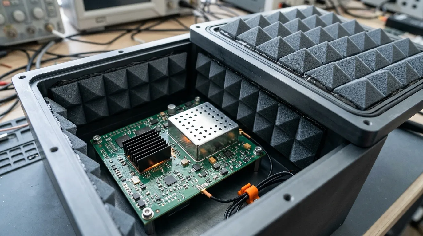
Placement follows from the field map rather than from symmetry. Covering the lid above the noisiest device, and the wall behind a connector or a heatsink stub, changes the Q of the modes that are actually being excited. Covering the whole interior is more effective and costs height, adhesive and assembly time. What does not work is a small patch in a corner chosen for convenience: partial coverage changes Q where it sits, and a cavity has more than one mode.
Antenna Isolation: What an Absorber Does Between Two Radiators
Two antennas on one board couple through three paths: direct radiation between them, surface and creeping currents travelling along the ground plane and chassis, and reflections from whatever the enclosure puts in the way. An absorber sheet placed between the two addresses the second path most directly, and partly the third.
The measurement is straightforward — drive one port, measure the other, with and without the part — and that number is an isolation figure in dB. What is not straightforward is the trade. An absorber close to a radiating element also absorbs the field you want: gain drops, efficiency drops, and the pattern can tilt. The practical rule is to keep the absorber out of the reactive near field of the main beam and put it where the unwanted energy travels — along the ground plane between the radiators, under the lip of a shield can, at the tip of a radome, or around the base of a monopole.
Surface currents are the reason this works at all. Travelling and creeping waves along a ground plane contribute to radar cross-section and to interference inside microwave modules, and a lossy sheet laid on that surface attenuates them before they reach the receive element. The same mechanism is why thin absorbers are used in antenna hats and test boxes, and why the requirements are different from a chamber lining: here the part must be thin, mechanically stable, and often non-conductive, because it sits within millimetres of live circuitry.
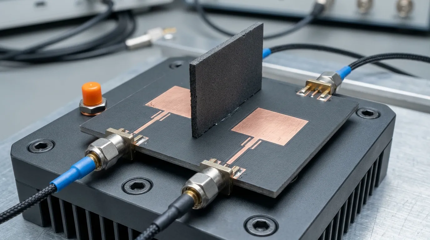
For arrays the problem shifts rather than disappears. Mutual coupling between elements changes the active impedance and distorts the pattern, and an absorber placed at the array edge or between sub-arrays is a common fix. As with a single pair, verify by measuring the coupled port rather than by trusting a band claim: the coupling you are trying to kill sits at a specific frequency, and the absorber has to be at its most lossy there.
Three Decibels That Are Not the Same Number
Most absorber datasheets lead with a dB figure. Before comparing two of them, establish which of three quantities you are looking at, because they cannot be converted into each other.
Attenuation ranks how lossy a material is. Reflection loss describes a metal-backed sample. Insertion loss describes a path. Only the second and third are measurements, and neither can be derived from the first.
Attenuation, in dB/cm, is the rate at which a wave decays while propagating through the material. It is not measured directly; it is calculated from the complex permittivity and permeability, and it assumes the material fills all space. It is useful for ranking how lossy one compound is against another, and it is the number most often quoted in material-only tables. One datasheet puts it plainly: attenuation is a figure of merit for lossiness and should not be used to directly estimate insertion loss — a flexible silicone absorber sheet states it in those words — and manufacturer literature warns against using it to predict reflectivity. A datasheet that gives only dB/cm has told you about the filler, not about your board.
Reflection loss, in dB, is measured against a metal reference. The industry-standard fixture is the NRL arch: a transmit and receive antenna aimed at a metal plate, a calibration that sets the plate reflection as 0 dB, then the sample placed on the plate and the returned signal measured. A standard 2–18 GHz setup uses a sample of roughly 300 mm square at an antenna-to-plate distance of 760–900 mm. The arch, waveguide and reflectometer methods were codified for chamber linings in IEEE Std 1128, which covers 30 MHz–5 GHz and is written for absorber linings on a metal surface; it was placed on inactive-reserved status in 2023 with a revision in progress, and the 2–18 GHz arch practice above comes from manufacturer application notes like the one cited earlier rather than from that standard. What the number does tell you is how much energy a metal-backed sheet will stop from coming back — the right figure for cavity damping and surface-current suppression.
Insertion loss, in dB, is measured between two antennas facing each other: establish the 0 dB reference with nothing in the path, insert the sample, measure again. It captures reflection plus transmission in one figure. It is the right number when the absorber sits between a source and a victim, and it is the number that cannot be inferred from attenuation, because a thin high-loss sheet and a thick low-loss sheet can post the same insertion loss with completely different reflection behaviour.
A related trap is the resonant absorber. Many thin RF absorbers are quarter-wave devices: a narrow band of high absorption at a frequency set by permeability and thickness, and a band above it where the part behaves like a conductor. That is a feature, not a defect — it buys 20 dB or more in a narrow band at a thickness a broad foam lining could never fit — but it means the datasheet's best number belongs to one frequency, and your failing frequency has to be inside it.
One more pair of numbers is worth asking for even though it rarely appears on a product page: complex permittivity and permeability, with their loss tangents. Together they predict both the attenuation and how badly the part will mismatch the wave at its surface. When two suppliers quote the same dB at the same frequency with different thicknesses, these are the numbers that explain the difference — and the ones to demand in any RF absorber material datasheet.
The Seven Specs That Decide Whether It Works
Work through these in order. The first three eliminate most wrong parts; the last four decide whether the right part survives production.
1. Frequency band — the failing band, not "broadband". Start from the failing spectrum or the coupling measurement, not from the catalogue. A part specified 10 MHz–6 GHz and a part specified 12–18 GHz are not better or worse, they are different tools. If the noise is broadband, cover the dominant failing band first.
2. Attenuation at that band, and how it was measured. Ask for reflection loss on a metal-backed sample or insertion loss in a two-antenna setup, and ask at what angle of incidence. A number without a method is not comparable with any other number, including the one in your previous project's report.
3. Thickness, and the height you can spare. For a magnetic microwave absorber, increasing thickness shifts absorption downward in frequency; for a quarter-wave type, thickness is set by the design frequency. Both interact with permeability, so the datasheet's frequency–thickness map beats any rule of thumb. In a tight stack the compressed thickness after assembly is the number that matters, and compression changes the electrical thickness — the same discipline described in our guide to thermal pad thickness and compression.
4. Surface resistivity. A near-field absorber often sits directly on or beside components, and it must not conduct. Carbon-loaded foam is conductive by design; magnetic elastomers are typically insulating. A datasheet that gives surface resistivity in MΩ/□ — typical dielectric absorber sheets quote values in the hundreds of MΩ/□ — has told you whether the part can touch a live trace, and one that omits it has left the question open.
5. Temperature and power handling. Absorbed energy becomes heat in the part itself. In a high-field location — near a power amplifier, inside a cavity that is driven hard — the absorber's own temperature rise sets the limit. Check the maximum service temperature, and ask at what field strength the part was tested.
6. Flammability and substance compliance. Most telecom, automotive and consumer enclosures commonly specify a UL 94 V-0 rating, which means the specimen stops burning within about ten seconds of the flame being removed, and buyers should be checking the yellow card for the specific grade rather than the family name. Halogen-free, RoHS and REACH statements belong in the same conversation. The difference between the flame ratings that appear on absorber and pad datasheets is covered in UL 94 V-0 versus VTM-0.
7. Mounting and format. Pressure-sensitive adhesive is the default and it adds thickness, a dielectric layer and a shelf-life question. Mechanical retention avoids the adhesive but needs clearance. Die-cut tolerance decides whether the part lands where the simulation put it, and a converter that can hold tolerance on a 0.03 mm sheet is a different supplier from one that cuts foam — the process side is described in die-cutting for thermal pads and gaskets.
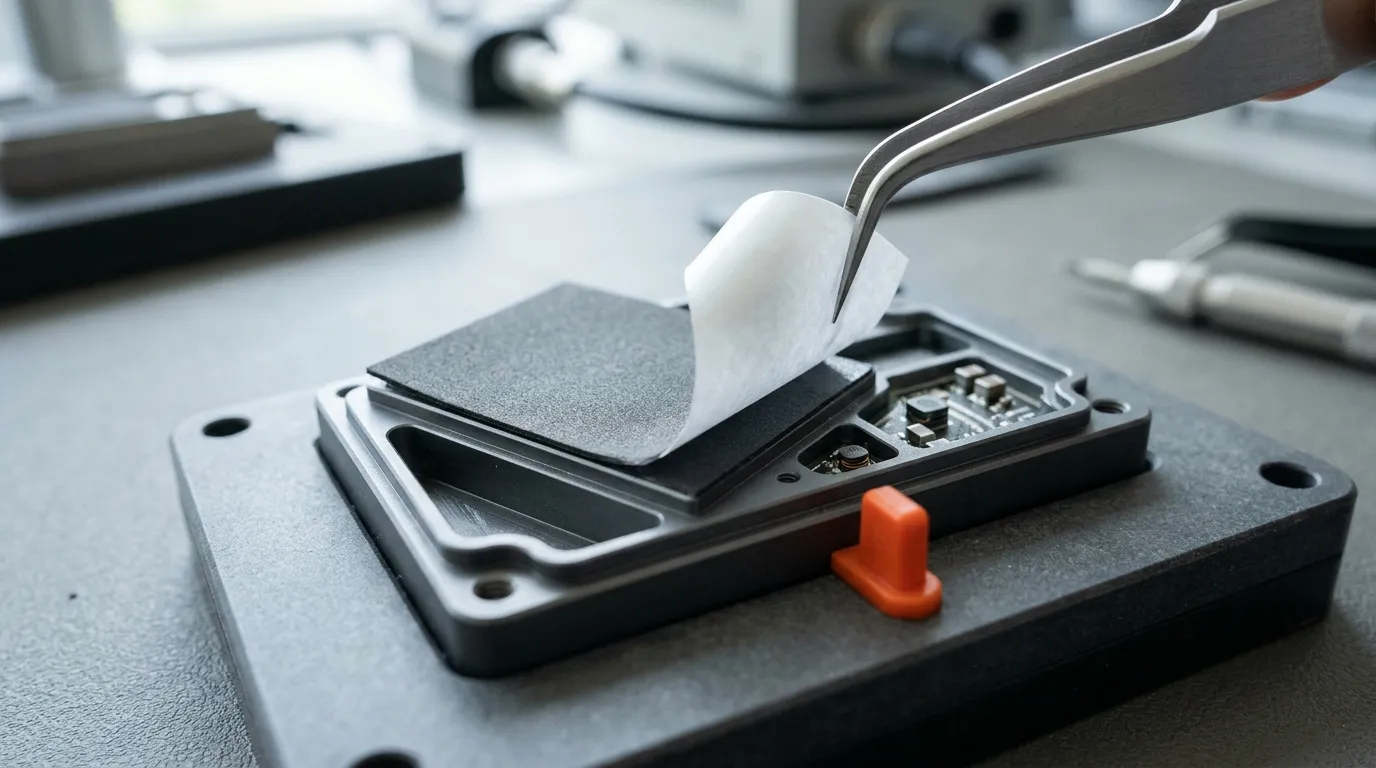
Our own line shows how that checklist maps onto part numbers — the TIR900 absorbing families and the thermal TIF900 — and where the list of specs runs out. Read the table from your constraint inward rather than from the catalog outward:
| Your constraint | Start with | Thickness to allow | What it is tuned for |
|---|---|---|---|
| Noise falls in 10 MHz – 6 GHz | TIR930-A to TIR9200-A | 0.03–0.50 mm | High-permeability magnetic sheet (µi 30–200 at 1 MHz); thin enough for tight stacks |
| Noise falls in 2 – 12 GHz | TIR-GC | 0.50–2.00 mm | Wider band, bought with thickness |
| Noise falls in 12 – 18 GHz | TIR-HK | 0.50–2.00 mm | Upper band; same thickness window as GC |
| Heat has to leave through the part | TIF900 (-15S to -40F) | 0.5–12 mm | Absorbing plus thermal: 1.5–4.0 W/mK, −45 to 200 °C, halogen-free |
The two 2–18 GHz classes are not a menu of equal options: what separates them is which half of the band the part is tuned into, and that is the question to put to a supplier before a sample ships. Those are series-level typical values, not a promise for a part number: the grade you order carries its own curve, and the band edges are where that curve is at its worst. The same logic applies to the combined thermal and absorbing class, where the trade-offs between heat path and absorption are the subject of the thermal conductive + EMI absorbing materials guide.
How to Qualify an RF Absorber on Your Own Board
The datasheet narrows the field; the board decides. Four steps, in this order, will settle it faster than any further reading.
Locate the source before choosing the part. A near-field probe and a spectrum analyser will show which device, seam or cable is radiating, and at which frequency. Without that map you are choosing a band by guesswork, and a cavity has several modes.
Run an A/B test with the part in the intended location. For near-field problems, quote the result in the terms IEC 62333-2 and its 2015 amendment define, so that two suppliers' numbers can be compared at all: the intra-decoupling ratio (Rda) — source and victim on the same side of the sheet, coupling measured before and after it goes in — the inter-decoupling ratio (Rde) with them on opposite sides, the transmission attenuation power ratio (Rtp) along a microstrip line, and the radiation suppression ratio (Rrs), which is how much less the board radiates once the sheet is fitted. The amendment adds a fifth, the line-decoupling ratio (Rdl). Commercial absorber literature quotes these ratios by name; a supplier who says only "attenuation" has not told you which one, and the microstrip measurements (Rtp and Rrs) are the closest analogue to a real board.
For radiated problems, measure in the chamber or on the OATS, not on the bench. Absorbers change the field distribution, so a bench measurement with a hand-held probe can show an improvement that disappears once the enclosure is closed. Compare a full scan with and without the part, at the same orientation, and watch for new peaks appearing at other frequencies.
Write the method into the drawing. The purchase specification should name the band, the attenuation figure and its test method, the thickness and its tolerance, surface resistivity, flame rating, and the adhesive. A part number alone delegates all of that to the supplier's interpretation, and that is how two builds of the same board end up with different EMC results.
Five Mistakes That Show Up in Failed Builds
- Comparing dB across methods. A 20 dB/cm attenuation figure, a −20 dB reflection loss and a 20 dB insertion loss are three different claims, and the numbers happen to look alike. Ask for the method every time.
- Ignoring the band shift from thickness. A resonant part specified at 1.0 mm does not stay at its design frequency when the stack compresses it to 0.8 mm. Specify the compressed thickness and the tolerance together.
- Putting a conductive absorber on live circuitry. Carbon-loaded foam attenuates well and conducts. If the part touches a trace or a component lead, the failure mode is electrical, not electromagnetic.
- Treating adhesive as free. PSA adds a dielectric layer and height, and it limits rework. In a stack that was tuned without it, adding tape moves the electrical distance to the ground plane.
- Forgetting that an absorber is also a thermal part. Where the absorber sits between a hot device and a heat sink, its thermal resistance joins the stack. The absorbing and heat-spreading functions can be combined in one material, but only if both are specified.
Sourcing: What to Ask Before You Commit
Six questions separate a supplier who knows the material from one reselling a catalogue entry:
- Which band does this grade cover, and can I see the reflection loss or insertion loss curve across it?
- How was that curve measured — NRL arch, waveguide, or two-antenna insertion loss — and at what incidence angle?
- What is the surface resistivity, and is the part safe in contact with circuitry?
- Which UL 94 rating applies to this specific grade, and is it on the yellow card?
- What is the compressed thickness tolerance after a die-cut and PSA build?
- Can you supply samples in the exact thickness and die-cut shape, with the adhesive I will use in production?
The last question is the one that shortens qualification most. An RF absorber is cheap relative to a failed EMC retest; the cost is in the iteration. ZIITEK supplies absorber sheets and combined thermal-absorbing pads across the TIR900 and TIF900 families, die-cut to drawing with documented tolerances, and can quote against a failing spectrum rather than a generic band — the thermal pad and thermal material range is the place to start, or send the scan and the mechanical envelope to the engineering team.
Emissions limits, exposure limits and flame ratings are all fixed by standards you do not control; the absorber is one of the few variables you do. Choosing it by frequency, by measurement method and by mounting — rather than by the biggest dB on the page — is what turns a part number into a fix.