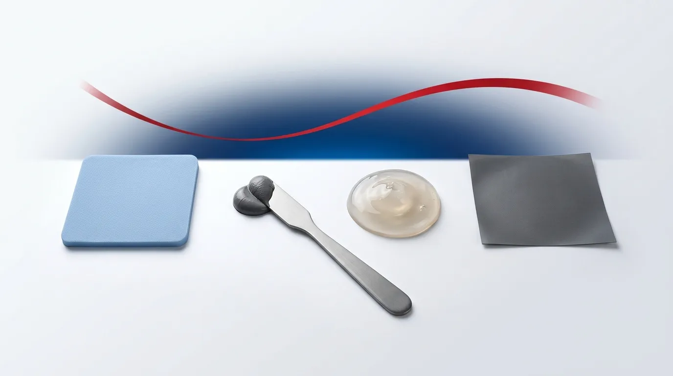
How to Choose a Thermal Interface Material
Choosing a thermal interface material means matching W/mK, thickness, hardness and insulation to your gap and power budget. A step-by-step guide for engineers.
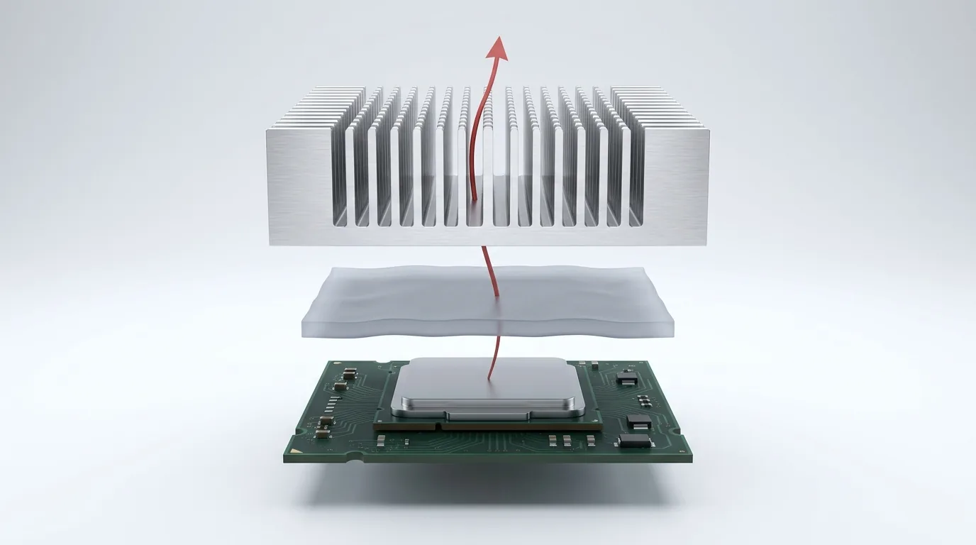
To choose a thermal interface material (TIM), match four properties to your design: thermal performance (thermal impedance, not just W/mK), the gap size and its tolerance, the mounting pressure your assembly allows, and whether the material must electrically insulate. Get those right and the material type — paste, pad, gel, or phase change — mostly chooses itself. This guide gives you the decision framework in the order a design engineer actually works, with the numbers that let you defend the choice.
Most “how to choose a TIM” articles are catalogs: here are the types, here are their W/mK, pick one. That is not a selection method — it’s a menu. Below is the method. For the full landscape of material types, start with the thermal interface materials selection guide; this article is about deciding.
ZIITEK has manufactured thermal-management materials since 2006 and ships gap pads, gels, greases, phase-change materials and carbon-fiber pads to OEMs across EV, datacenter, telecom, LED and industrial markets. The framework below reflects what we see specified — and re-specified after it fails — at production volume.
Step 1 — Start with the joint, not the material
The single most common mistake is choosing a material by its headline conductivity before understanding the joint it has to fill. Before you look at any datasheet, characterize the interface:
- Gap size and tolerance. Is it a near-zero contact (a lapped CPU lid on a cold plate) or a real, variable gap (a tall component under a lid, 0.5–5 mm)? Measure it across several units — the tolerance stack-up often matters more than the nominal, and Step 8 shows exactly how it can overturn a material choice.
- Flatness and roughness of both surfaces.
- Power to dissipate, the contact area it flows through, and the allowable temperature rise (your junction-temperature budget).
- Mounting method and pressure. Screws with springs, clips, or adhesive? How much force can the component and PCB survive?
- Environment. Operating temperature range, thermal cycling, vibration, humidity, and any outgassing or flammability constraints.
Those five answers eliminate most of the catalog before you compare a single W/mK.
Step 2 — Set the performance you actually need
Do not buy conductivity you cannot use. What determines the temperature drop across the joint is thermal impedance (°C·cm²/W or °C·in²/W) at your real thickness and pressure — a combination of bulk conductivity and the contact resistance at each surface. Per unit area:
R″ ≈ BLT / k + R″contact
where BLT is the bond-line thickness — the thickness the material actually ends up at in the assembly, not the thickness on the box. The whole reason a TIM exists is that the alternative is air, at roughly 0.026 W/m·K; even a mediocre TIM is two orders of magnitude better, but only across the area it genuinely touches.
That second term is why a well-conforming 6 W/mK material can beat a stiff 12 W/mK one that never wets out — and why you should compare candidates on impedance measured to ASTM D5470 at a stated pressure and BLT, not on headline W/mK alone. A vendor who publishes only a W/mK number is handing you the easy half of the equation.
It also explains why two pads with identical W/mK can behave differently: conductivity comes from the filler. Ceramic fillers (boron nitride, alumina, aluminum nitride, zinc oxide) conduct heat while staying electrically insulating; metal fillers (silver, copper) and liquid metal push conductivity far higher but conduct electricity too. The filler loading that buys you W/mK is also what makes a pad stiffer — which becomes Step 5’s problem.
Estimate the impedance budget from your heat load, contact area and temperature margin, then shortlist materials that meet it at the thickness and pressure you can achieve. If W/mK and impedance sound interchangeable to you, read understanding thermal conductivity (W/mK) in TIM and thermal resistance vs thermal impedance first — this is the step engineers most often get wrong.
Step 3 — Let the gap pick the form factor
The gap and its tolerance narrow the material type faster than anything else. The matrix below maps the joint to a material class, with the ranges we actually ship so you can sanity-check a shortlist before requesting datasheets:
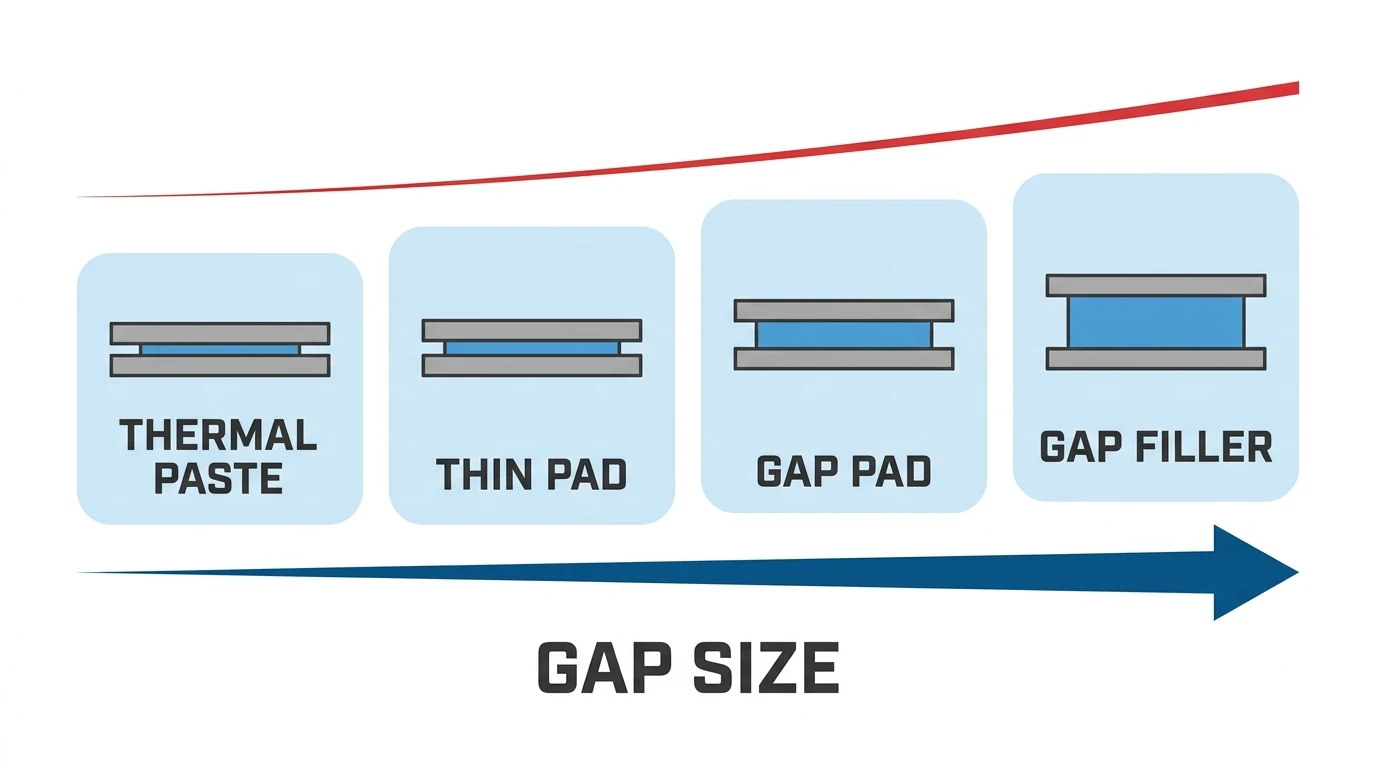
| Interface | Best-fit class | Typical W/mK | Serves what gap | Hardness | Electrical |
|---|---|---|---|---|---|
| Near-zero, flat, high-power (CPU/GPU lid) | Thermal paste (TIG®780) | 1.0–5.2 | Bond line down to tens of µm | Liquid — no compression force | Not a rated insulator |
| Near-zero, flat, thermally cycled | Phase change (TIC®800) | 0.95–9.6 | Thin film; flows above T-phase 50–60 °C | Solid cold, conforms hot | Not a rated insulator |
| Small, defined gap; insulation; volume assembly | Gap pad (TIF®) | 1.25–18 | ~0.5–5 mm | Shore 00 (soft) to Shore A (firm) | Dielectric silicone |
| Isolation is the primary job | Insulating pad (TIS®) | 1.0–1.6 | Thin, defined | Firm | 1500–6000 VAC rated |
| Large or highly variable gap, low stress on parts | Gap filler / gel (TIF® gel) | 1.5–9.0 | Conforms to any gap; no fixed nominal | Uncured — near-zero stress | Dielectric silicone |
| Ultra-thin, high conductivity, non-insulating | Carbon-fiber pad (TIR®700) | 9–35 | Thin, low pressure | Soft | Electrically conductive |
| Highest conductivity, non-insulating | Liquid metal | 35–58 | Very thin | Liquid | Conductive — never near live traces |
Two things fall out of this table immediately. The high-W/mK options (carbon fiber, liquid metal) are the ones that cannot insulate, so Step 4 often deletes them before performance is even discussed. And a gap filler is the only class with no nominal thickness to get wrong — which matters more than it sounds, as Step 8 demonstrates.
Step 4 — Check the electrical requirement
This is a hard gate, not a preference. If the TIM sits between a component and a grounded heatsink where a short would be catastrophic, you need a dielectric material.
Three rules keep this from going wrong:
- Read the breakdown voltage, not the thermal spec. Insulation is a property of the polymer and filler system, and nothing about a W/mK number tells you whether the material isolates. A dedicated insulating grade such as TIS® is rated 1500–6000 VAC precisely because that is the number the design has to be defended against.
- Design in margin, and remember the rating is thickness-dependent. A breakdown-voltage rating belongs to a material at a stated thickness. Compress it thinner and the isolation falls with it — so the worst case to check is the thinnest point of the assembly under maximum clamp, not the nominal.
- Know when the joint wants the opposite. If the design needs an electrical path for grounding or EMI, a carbon-fiber or metal-loaded material is correct — and a dielectric pad is the failure.
The trap is that the highest-conductivity materials in Step 3’s matrix are conductors. A 35 W/mK carbon-fiber pad is an excellent answer to a thermal problem and a dead short across a live trace.
Step 5 — Match hardness and mounting pressure
For pads and gels, softer usually wins. A soft material conforms to both surfaces under low pressure, wetting out to cut the contact-resistance term from Step 2 and protecting fragile dies and BGA solder joints. A hard, high-filler pad may boast higher bulk W/mK yet perform worse because it never fully contacts the surfaces — and it over-stresses the component while it fails to.
Hardness is quoted on two different ASTM D2240 scales, and confusing them is a real sourcing error:
- Shore 00 — the scale for soft gap pads and gels. Lower number = more conformable at low pressure.
- Shore A — the scale for firmer elastomers. The scales are not interchangeable: a material quoted on Shore A is in a different class of stiffness from one quoted on Shore 00, and comparing the bare numbers across scales is meaningless.
The number that actually decides it is neither, though — it’s deflection force: how much pressure the datasheet says it takes to compress that pad to your target thickness, versus how much force your clip or screw actually delivers. A pad that needs more force than the assembly can apply will never reach its rated impedance, and the joint runs hot at the exact W/mK you paid for. Ask for the compression-force-vs-deflection curve; if a vendor cannot supply one, you cannot size the joint. Thickness, compression ratio and deflection force are a linked decision — the full method is in the thermal pad thickness & compression guide.
Step 6 — Confirm reliability and compliance
The material has to survive the product’s life, not just the first thermal test:
- Thermal cycling. The two surfaces expand at different rates (differential CTE), working the joint every cycle. In pastes this drives pump-out and dry-out; in pads it drives compression set — the pad takes a permanent set, stops pushing back, and the contact pressure you designed around quietly disappears. Delamination is the end state of both.
- Operating temperature range across the real environment, not the bench.
- Outgassing — low-volatile or silicone-free grades near optics and sensors.
- Flammability — UL 94 V-0 for most electronics.
- Regulatory — RoHS, REACH, and any automotive (IATF 16949) or medical requirements for your market.
A material that passes bench testing but fails these is a field-return waiting to happen — and compression set is the one that fails silently, because nothing looks wrong until the joint is already hot.
Step 7 — Optimize for manufacturability and volume economics
The best-performing material is not automatically the right one. At volume, application method and yield dominate cost: a die-cut pad or an automated dispense of gel can be far cheaper and more repeatable than hand-applied paste, even at a higher unit price. Consider format (sheet, die-cut, adhesive-backed, dispensable), placement cycle time, rework, and scrap. Die-cut parts also carry a thickness tolerance of their own — one more band to add to the stack-up you measured in Step 1.
The decision framework, in one pass
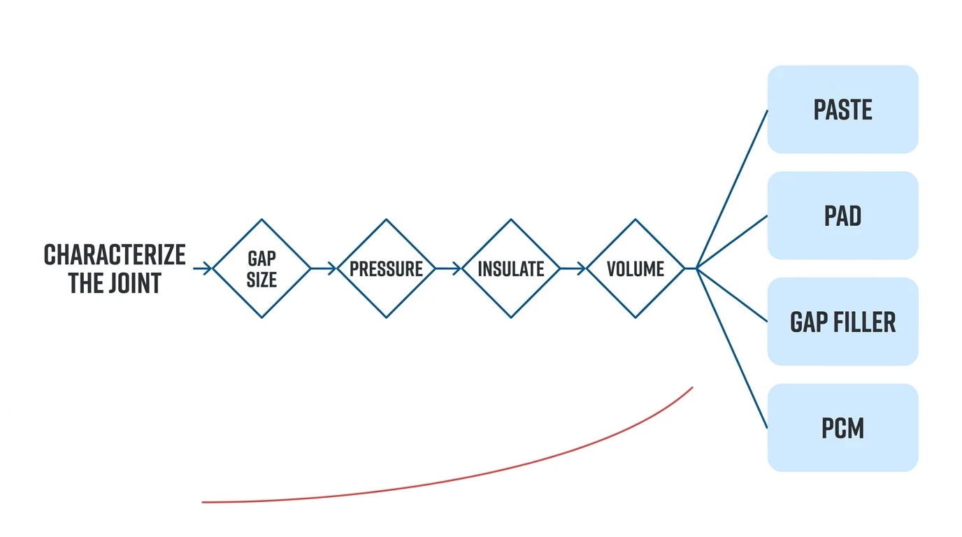
- Characterize the joint (gap, tolerance, flatness, power, area, pressure, environment).
- Set the thermal-impedance budget — target impedance at your BLT, not headline W/mK.
- Let the gap pick the form factor.
- Apply the electrical gate (insulate vs conduct; check breakdown voltage at the thinnest point).
- Match hardness to mounting pressure (deflection force vs available clip force).
- Verify reliability + compliance (cycling, compression set, outgassing, UL, RoHS/REACH).
- Optimize for manufacturability at your volume (format, dispense, yield).
Work them in order and the shortlist usually collapses to one or two materials you can then sample and validate.
Step 8 — A worked example: when the tolerance kills the pad
A 40 W power module dissipates through roughly 20 cm² of contact area. It sits 1.5 mm under a lid, the gap measures ±0.3 mm across units, it sits near live traces, and it is assembled at 50k/year with clip pressure only.
Steps 1–4 are quick. Real, variable gap → not paste. Insulation required → dielectric, which deletes the carbon-fiber and liquid-metal rows. Low clip pressure → must be soft. Everything points at a soft silicone gap pad. So size one.
The pad has to hold 20–30% compression across the whole tolerance band, not just at nominal. Compression is (t − gap) / t for a pad of nominal thickness t, and the band is 1.2–1.8 mm:
- At the maximum gap (1.8 mm) the pad is least compressed. For ≥20% there:
t ≥ 1.8 / 0.80 =2.25 mm. - At the minimum gap (1.2 mm) it is most compressed. For ≤30% there:
t ≤ 1.2 / 0.70 =1.71 mm.
t ≥ 2.25 mm and t ≤ 1.71 mm cannot both be true. No single pad nominal serves this joint. The intuitive pick — a 2.0 mm pad, “about 20–30% into a 1.5 mm gap” — actually delivers 40% compression on the tight units (crushing a fragile module at clip force) and 10% on the loose ones (barely touching, running hot). A ±0.3 mm band on a 1.5 mm gap is simply wider than a 20–30% window can absorb. That is Step 1’s warning made arithmetic: the tolerance mattered more than the nominal, and it overturned the material class.
So the answer is the class with no nominal to get wrong: a dispensed gap filler. It conforms to whatever each unit’s gap turns out to be, at near-zero stress on the part, and it dispenses automatically at 50k/year. Checking it against the Step 2 budget, for a TIF® gel at 3 W/mK and a 1.5 mm bond line:
R″ = BLT / k = 0.0015 m ÷ 3 W/mK =5.0 × 10⁻⁴ m²·K/W, i.e. 5.0 °C·cm²/W- Over 20 cm²:
R = 5.0 ÷ 20 =0.25 °C/W ΔT = 40 W × 0.25 °C/W =10 °C across the joint, plus a small contact term a well-wetting gel keeps near zero.
A 10 °C rise against your junction-temperature budget is a number you can defend in a design review — and none of it required the highest W/mK on the shelf. The answer wasn’t “the highest W/mK pad.” It wasn’t a pad at all.
When this framework doesn’t apply
Selection is not always an engineering decision, and pretending otherwise is how a guide like this loses credibility:
- The part is already qualified. If a material sits on an approved vendor list or inside a released automotive or medical qualification, re-qualifying it can cost more than the thermal margin is worth. The framework tells you what to spec on the next design.
- The customer specified it. In contract manufacturing the material is often dictated. The useful output is then a documented deviation request, not a better shortlist.
- A drop-in is the real requirement. Sometimes the actual ask is to match an incumbent material’s impedance, thickness and compression behavior closely enough to swap it without re-testing. That is a matching exercise against a datasheet, not an open selection.
- The gap is not the problem. If the heat sink is undersized or the airflow isn’t there, no TIM saves it. A TIM removes an interface penalty; it cannot remove heat the system was never able to reject.
Frequently asked questions
Is higher W/mK always better? No. Real cooling depends on thermal impedance at your actual thickness and pressure. A soft, well-wetting mid-W/mK material often beats a stiff high-W/mK one — and the highest-W/mK materials are electrically conductive, so they are disqualified outright wherever the joint must insulate.
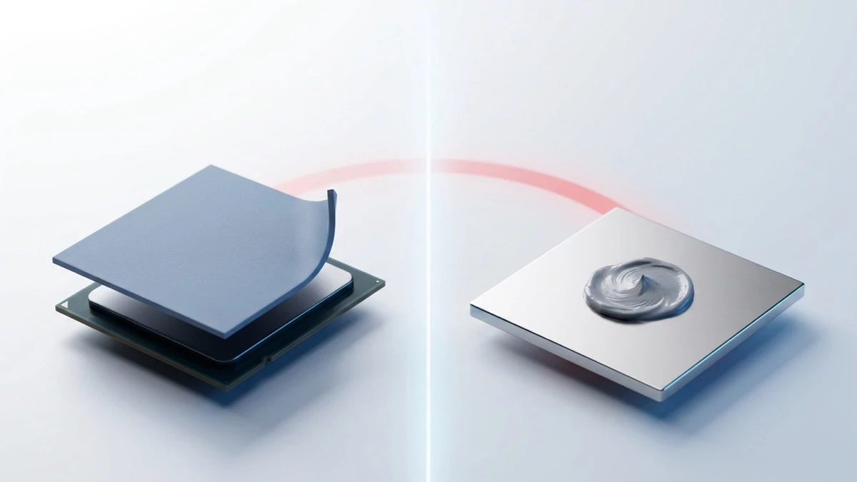
Paste or pad? Paste for flat, near-zero, high-power joints; pad for defined gaps, insulation, and volume assembly. See thermal pad vs thermal paste.
How do I choose thickness? Measure the gap and its tolerance, then check that a candidate nominal stays inside your compression window at both the minimum and the maximum gap. As Step 8 shows, a wide tolerance band can make every pad nominal illegal at once.
What if I need electrical isolation? Choose a dielectric material and verify breakdown voltage against your working voltage with margin, at the thinnest point of the assembly — never infer insulation from thermal specs.
What is the best thermal interface material? There isn’t one. The best material is the lowest-impedance option that fits your gap band, insulates if required, and compresses under the force you actually have — which is why the framework runs in that order.
Choosing with confidence — and support
A good TIM choice is defensible: you can name the impedance budget, the gap tolerance, the pressure, and the insulation requirement that drove it. If you’d rather validate against real parts, ZIITEK’s engineering team can shortlist grades across paste, pad, gel, and phase change to your joint and send samples — the fastest way to close out steps 1–8 with data instead of a datasheet guess.
Further reading: DuPont/Laird, “How to Choose the Right Thermal Interface Materials” (PDF); Mouser, “Selection Guide: Thermal Interface Materials” (PDF).